EE 330 Lecture 2026 11 03 Ch7 Amp#1
Overview
The lecture develops small-signal amplifier analysis from MOSFET and BJT operating regions through equivalent-circuit models and worked circuit-reduction methods. It derives the common-source and common-emitter gain relationships, shows how biasing and coupling or bypass capacitors separate DC operation from AC signals, and introduces the BJT parameters g_m = I_C/V_T and r_π = β/g_m.
Key takeaways
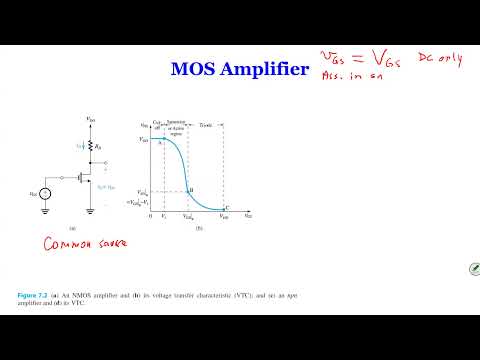
- A common-source MOSFET amplifier in saturation has small-signal gain approximately -g_mR_D, where g_m = 2I_D/V_OV; the negative sign means 180-degree phase inversion.
- A common-emitter BJT amplifier has gain approximately -g_mR_C, with g_m = I_C/V_T and V_T approximately 25 mV.
- The basic MOSFET small-signal model has an open gate and a controlled current source g_m v_gs, while the BJT model adds base-emitter resistance r_π = β/g_m.
- AC analysis replaces DC voltage sources with ground and DC current sources with open circuits; sufficiently large capacitors become AC shorts but remain open circuits for DC.
- A source or emitter resistor can support DC bias stability while a parallel bypass capacitor reduces its AC effect, separating bias design from signal gain.
- For BJT circuits, emitter impedance reflects to the base multiplied by approximately β + 1, enabling complex input networks to be reduced before calculating v_be and output.
Chapters
- Students may discuss concepts together, but each individual project requires a separate circuit drawing, simulation, graph, and write-up.
- MOSFETs dominate many modern integrated circuits because their gates require negligible drive current; BJTs remain in products such as the LM324.
- The lecture contrasts low MOSFET turn-on thresholds, cited as roughly 0.2 to 0.3 V for some designs, with the BJT's typical 0.7 V base-emitter turn-on.
- The chapter moves from transistor operation to small-signal models, then revisits common-base, common-emitter, common-source, and common-drain configurations.
- DC biasing sets the operating point and usable signal range; poor bias choices can reduce range or require unnecessary components.
- Discrete amplifiers add capacitors to separate DC bias from AC signals, preparing for later amplifier designs including Class A, B, AB, C, and D.
- For amplifier operation, the lecture identifies MOSFET saturation and BJT forward-active operation as the desired regions, while warning that 'saturation' means different things for the two devices.
- A MOSFET must have V_GS above threshold and V_DS at least as large as the overdrive voltage V_OV = V_GS - V_T to remain in saturation.
- A BJT typically needs V_BE around 0.7 V and V_CE above roughly 0.3 V for active operation; V_CE below that boundary indicates saturation.
- The DC BJT collector current follows I_C = I_S exp(V_BE/V_T), with thermal voltage V_T approximately 25 mV.
- Capital voltage symbols such as V_GS denote the DC bias, lowercase v_gs denotes the small AC signal, and the total signal is their sum.
- The total gate-source voltage is written v_GS = V_GS + v_gs, distinguishing the operating point from the input variation.
- Small-signal analysis assumes the AC variation is small enough that the transistor remains in its intended operating region.
- For a MOSFET in saturation, the lecture uses I_D = 1/2 k_n(V_GS - V_T)^2 as the DC current relation.
- Substituting V_GS + v_gs and neglecting the squared small-signal term yields i_d = g_m v_gs, where g_m = k_n(V_GS - V_T) = 2I_D/V_OV.
- With drain resistor R_D, the AC output is v_o = -g_m R_D v_gs, so the common-source stage inverts the signal by 180 degrees.
- The negative gain follows because an increase in gate signal increases drain current and produces a larger voltage drop across R_D.
- A series output capacitor blocks the drain's DC level from reaching the load while allowing AC output to pass.
- The capacitor's impedance magnitude is 1/(ωC); sufficiently large capacitance at the signal frequency makes the AC impedance small.
- The common-source gain remains approximately -g_mR_D when the coupling capacitor passes the signal with little attenuation.
- The MOSFET small-signal model represents the device with a controlled drain current source g_m v_gs and an open gate input.
- External R_D converts the controlled current into an output voltage, giving the familiar inverting common-source gain.
- For AC analysis, independent DC voltage sources such as V_DD are replaced by ground; DC current sources are opened.
- The transistor model contains the device's small-signal behavior, while resistors such as R_D remain external circuit elements.
- The worked circuit is reduced by replacing the MOSFET with its g_m v_gs current-source model and reconnecting every component at the gate, source, and drain.
- Large capacitors C1 and C2 are treated as AC short circuits when 1/(ωC) is negligible.
- Gate-bias resistors R_G1 and R_G2 both connect to AC ground because V_DD becomes ground in the small-signal model.
- A source resistor R_S makes v_gs differ from the input v_in; treating them as equal is incorrect unless the source is at AC ground.
- A source resistor can stabilize the DC operating point while a capacitor placed in parallel with it provides a low-impedance AC path.
- When the bypass capacitor is large enough that 1/(ωC) is small, the source becomes approximately AC-grounded.
- An inductor placed in series does not provide the same AC bypass function; the lecture emphasizes placing the bypass capacitor in parallel with the resistor.
- The BJT derivation starts from I_C = I_S exp(V_BE/V_T) and adds a small base-emitter signal v_be to the DC bias V_BE.
- Using a first-order Taylor expansion for small v_be gives i_c = g_m v_be, with g_m = I_C/V_T.
- At V_T ≈ 25 mV, the BJT's transconductance is set by its DC collector bias current.
- With collector resistor R_C, the common-emitter output is v_o = -g_mR_Cv_be, an inverted AC signal like the common-source result.
- Unlike the MOSFET gate, the BJT base draws current, so the small-signal model needs an input resistance between base and emitter.
- Using i_b = i_c/β and i_c = g_m v_be gives i_b = v_be/r_π, where r_π = β/g_m.
- The BJT equivalent circuit therefore includes both the controlled collector current source g_m v_be and r_π; the MOSFET model has no corresponding gate resistor in this basic model.
- The controlled source and r_π belong to the transistor model, while R_C and the signal source are external.
- The circuit-reduction exercise replaces the BJT with its g_m v_be source and r_π, then reconnects the surrounding input, bias, emitter, and collector networks.
- The DC collector current I_C determines g_m = I_C/V_T, and β together with g_m determines r_π = β/g_m.
- V_CC becomes AC ground, while the input source, source resistance, coupling capacitors, bias resistors, and load remain in the AC network.
- The output load R_L connects through the collector coupling capacitor, and R_C connects from the collector side to AC ground.
- At finite frequency, coupling and bypass capacitors contribute impedance 1/(jωC), causing both voltage attenuation and phase shift.
- The emitter network combines R_E1 in parallel with R_E2 + 1/(jωC3); a sufficiently large C3 makes the bypass branch's AC impedance small.
- Splitting emitter resistance allows DC bias stability and AC gain to be adjusted separately, for example by pairing a larger unbypassed resistor with a much smaller bypassed resistor.
- The lecture suggests solving complex networks analytically, with SPICE, or with MATLAB matrix equations.
- The input network can be simplified to R_S' = R_S + 1/(jωC1), while the base-bias resistors combine as R_B = R_B1 || R_B2.
- The collector network becomes R_L' = R_C || [R_L + 1/(jωC2)], reducing the number of elements in the AC model.
- These equivalent impedances turn the original multi-capacitor circuit into a simpler network around r_π, the controlled current source, and the emitter impedance.
- Because i_e = i_c + i_b = (β + 1)i_b, an emitter impedance Z_E appears at the base as approximately (β + 1)Z_E.
- The base-side equivalent must retain r_π in series with the reflected emitter impedance; incorrectly placing r_π and Z_E directly in parallel gives the wrong result.
- After combining the input divider, calculate v_be, then i_c = g_m v_be and v_o = -i_cR_L'.
- The lecture closes with a repeatable sequence: simplify impedances, solve the base-emitter signal, find collector current, and determine output voltage.
Transcript excerpt
0:00 In this class we're doing all individual projects. And then it doesn't prevent you guys from talking to each other, you know, or even working together on some of the major, you know, issues, discussions, understanding the basic concepts and so on. But but at the end of the day you got to try you got to draw your own circuit, do your own simulation, attach your own graph, your own write up. That's all you need. >> I have a question. When would you want to use a BJT versus a MOSFET? >> When would you use a BJT versus a MOSFET? Um Well most of the time that will be a design it's a preference of the designer.
0:48 And for integrated circuits, in fact it's it's mostly MOSFETs now. BJT is rarely used. BJT is like a legacy product. And still if you buy say a LM324 op-amp, this still uses BJTs. Very good product, very cheap. So basic functions. And then the advantage is that as you can see from chapter five and six, MOSFET does not need any current to drive the circuit. A BJT does. Right? So MOSFET can have a lower voltage because it's a threshold voltage. It can go lower with all the newer designs of the MOSFET like a depletion type and so on. You sometimes you get really low like 0.2, 0.3 volts to turn on the MOSFET, but you need a 0.7 minimum to turn on the BJT.
1:38 So MOSFET definitely gains a lot of advantage on BJTs. All right. So now we have MOSFETs and BJTs uh the basic component, the basic operating principle and so on. So this chapter we're going to dive in how to use those devices as an amplifier. And this this this for this class, and in this chapter
This is the start of the transcript. Save this video free for the whole transcript, searchable and time-coded.
In this course
Related notes
Summary, takeaways, and chapters were generated by AI from the video's transcript and may contain errors. The video belongs to its creator, Wireless Power Transfer.