EE 330 Lecture 2026/10/01 Ch5 MOS#1
Overview
The lecture introduces n-channel and p-channel MOSFETs, explaining how a gate voltage across silicon dioxide creates a surface channel and how channel geometry and overdrive voltage control drain current. It develops the linear/triode and saturation operating regions, their I-V equations, pinch-off, and CMOS complementarity, with examples using a 0.18-micrometer process and a 4-nanometer oxide.
Key takeaways
- An nMOS gate does not conduct through its oxide in steady state; its electric field induces an electron channel at the silicon surface between the source and drain.
- Gate overdrive VOV = VGS - VT controls channel strength, while the ratio W/L and parameter k'n = μnCox scale the MOSFET’s current.
- In the triode region, ID = k'n(W/L)[VOVVDS - VDS²/2]; saturation begins near VDS = VOV, where the ideal current becomes 1/2 k'n(W/L)VOV².
- A MOSFET can act as a voltage-controlled resistor at small VDS, but channel narrowing near the drain makes the current nonlinear as the device approaches saturation.
- The lecture’s fabrication example combines a 0.18-micrometer process, 4-nanometer oxide, 450 cm²/(V·s) mobility, and 0.5-volt overdrive to estimate a channel width near 0.93 micrometers for a 1-kilohm resistance.
- CMOS logic pairs nMOS and pMOS devices with opposite carrier and voltage polarities, enabling complementary switching in which one transistor conducts while the other is off.
Chapters
- Chapter 2, 4, 5, 6, and 7 bonuses can add up to 9 points beyond the 100-point course total.
- The lecture notes an October 29 midterm covering Chapters 5 and 6, and a tentative December 15 final worth 40 points.
- Late homework and project submissions receive automatic point deductions, so students are advised to track deadlines.
- Chapter 5 covers MOSFET operation, current-voltage characteristics, and DC circuit analysis; small-signal AC analysis is reserved for Chapter 7.
- The course plans four lectures on Chapter 5 and four on Chapter 6, which introduces bipolar junction transistors.
- The lecture emphasizes learning to apply MOSFET equations, with notes permitted during the exam.
- Conductors carry current through mobile electrons, while insulators such as rubber and ceramics have very few mobile carriers.
- Silicon is a semiconductor; doping it creates p-type material with holes or n-type material with additional electrons.
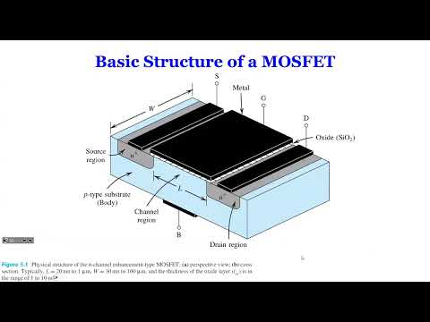
- The lecture uses p-type silicon as the MOSFET substrate and n+ regions as the source and drain.
- MOSFET means metal-oxide-semiconductor field-effect transistor, referring to the metal gate, silicon dioxide insulator, and semiconductor body.
- An nMOS structure places two n+ regions in a p-type substrate, with an oxide layer separating the gate from the silicon.
- The oxide prevents steady-state current from flowing directly between gate and substrate while allowing the gate voltage to establish an electric field.
- A positive gate voltage attracts electrons toward the silicon surface beneath the gate oxide, forming an inversion channel.
- Applying a drain-to-source voltage moves channel electrons between the n+ source and drain; conventional current flows in the opposite direction.
- The gate controls channel formation without requiring a direct conductive path through the oxide.
- Channel width W affects how much current the device can carry, while channel length L limits current as it increases.
- The threshold voltage VT is the gate-to-source voltage required to form a usable channel; the lecture gives roughly 0.3 to 1 volt as an illustrative range.
- Gate overdrive is VOV = VGS - VT, so increasing VGS above threshold strengthens the channel.
- The device parameter k'n is formed from electron mobility and oxide capacitance per area, commonly written k'n = μnCox.
- In the small-VDS linear approximation, ID is proportional to k'n(W/L)VOVVDS.
- The model captures the effects of semiconductor properties, oxide thickness, channel dimensions, gate overdrive, and drain voltage.
- For small VDS, drain current rises approximately linearly with VDS, allowing the MOSFET to behave like a voltage-controlled resistance.
- The lecture calls the low-VDS operating range linear and also uses the standard MOSFET term triode for the broader nonsaturation region.
- At fixed VGS, increasing VDS eventually invalidates the simple linear approximation as the channel narrows near the drain.
- A worked example uses a 0.18-micrometer fabrication process, electron mobility of 450 cm²/(V·s), and a 4-nanometer silicon dioxide layer.
- With VGS = 1 V and VT = 0.5 V, the example uses VOV = 0.5 V and a specified 1-kilohm channel resistance to estimate W at about 0.93 micrometers.
- The lecture describes Moore’s law as transistor count doubling about every 18 months and notes that scaling faces limits as dimensions approach nanometer scales.
- As VDS rises, the channel becomes narrower near the drain rather than remaining a uniform rectangle.
- The more complete triode equation is ID = k'n(W/L)[(VGS - VT)VDS - VDS²/2].
- The VDS-squared term accounts for channel narrowing and distinguishes the triode model from the small-VDS linear approximation.
- For a fixed VGS, the output characteristic plots ID against VDS, rising through the triode region before flattening into saturation.
- The transition occurs near VDS = VOV = VGS - VT; below this boundary the device is in triode, and above it the device is saturated.
- A family of output curves corresponds to different VGS values, with larger gate overdrive producing greater drain current.
- At the saturation boundary, the channel pinches off near the drain as the local gate-to-channel voltage falls to the threshold condition.
- The ideal saturation current is ID = 1/2 k'n(W/L)(VGS - VT)², which is approximately independent of VDS in the basic model.
- At fixed device geometry, increasing VGS raises saturation current because the equation depends on the square of gate overdrive.
- A pMOS uses an n-type body with p-type source and drain regions, reversing the carrier type and voltage polarities relative to nMOS.
- In pMOS devices, holes carry conventional current in the same direction as hole motion, unlike electron motion in nMOS.
- Complementary MOS, or CMOS, combines nMOS and pMOS so that one device can conduct while the other is off, a foundational arrangement for logic circuits.
- The final example asks for bias conditions that produce a specified saturation current and the minimum VDS needed for saturation.
- At the minimum saturation voltage, use the boundary condition VDS = VOV, then solve the saturation-current equation for VOV and recover VGS = VOV + VT.
- The lecture closes by previewing circuit-symbol analysis for nMOS and pMOS in the next class, replacing the physical cross-sections with schematic symbols.
Transcript excerpt
0:09 Who's as an aviation engineer. I was like, let me see. >> Okay. So, like I said, um uh I know the discount one wasn't average wasn't that high, but it's not too bad on average. So, we did give you uh bonus points that you can earn. So what it means that if you do all of
0:56 those bonuses chapter two, four, five, six and seven all total you would earn nine points total beyond 100. So your percentage is based on 100 but you can earn 109. So your final ABCD is based on the total but if you earn 90 or more out of 109 you will get a a minus right. So that's how it's calculated. So be sure do the bonuses. I it's it's yours if you don't do it. Uh I don't have a way to control who is doing it, who is not doing it. But takes the time to do it. You would earn. So those points are not reducing your total but actually adds to beyond 100. Does it make sense for everybody? I check a lot of student was confused how does it work? So basically the total is
1:43 100 for the car. If you don't do any bonus, if you don't do any bonus, you do perfect in every exam, you still get 100. You still get a but if you don't do well, like say if you do, if you do like 90% and you do all nine points, the bonus, you get a 99, you also get a A. Or if you do 70 in the class on everything else, but not the bonus, but you nine points of bonus, you get a C plus C minus. Does it make sense? you. Okay. >> So, those are the like free points for
This is the start of the transcript. Save this video free for the whole transcript, searchable and time-coded.
In this course
Related notes
Summary, takeaways, and chapters were generated by AI from the video's transcript and may contain errors. The video belongs to its creator, Wireless Power Transfer.