EE 330 Lecture 2026 11 16 Ch7 Amp#5
Overview
The EE 330 lecture derives voltage gain, input resistance, and output resistance for six MOSFET and BJT amplifier configurations: common source, common emitter, source- or emitter-degenerated versions, common gate, and common base. It uses small-signal π and T models to show how source resistance, emitter resistance, and input source resistance change gain, while ideal gate or base-current assumptions simplify resistance calculations.
Key takeaways
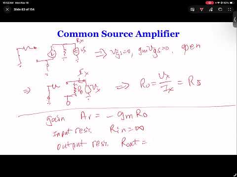
- An ideal common-source MOSFET stage has gain −gm·RD, infinite gate input resistance, and output resistance RD when transistor output resistance is neglected.
- A common-emitter stage’s gain from the input source is reduced by the Rsig-to-rπ divider, while its base input resistance is rπ and its collector output resistance is RC.
- Source degeneration changes common-source gain to −RD/(1/gm + RS); emitter degeneration raises common-emitter input resistance to rπ + (β + 1)RE while reducing gain.
- Common-gate and common-base stages have low input resistance, approximately 1/gm, and non-inverting gain; their ideal gains are RD/(Rsig + 1/gm) and α·RC/(Rsig + 1/gm), respectively.
- For output-resistance calculations, shorting the input often makes the controlling voltage zero, turning off the dependent current source and leaving RD or RC as the output resistance.
Chapters
- The common-source stage grounds the MOSFET source, applies the input at the gate, and takes the output at the drain.
- In the AC small-signal circuit, the DC supply becomes ground, placing drain resistor RD from the drain to ground.
- The MOSFET gate draws no small-signal current, so the input source resistor has no voltage drop.
- The drain current is gm·vgs, producing the inverting gain Av = −gm·RD.
- Because gate current is zero, the input resistance is ideally infinite.
- With the input shorted, the controlled current source turns off, leaving output resistance Rout = RD.
- The common-emitter stage grounds the emitter, drives the base through source resistance Rsig, and takes output at the collector through RC.
- The hybrid-π model adds rπ between base and emitter, and the collector current is gm·vbe.
- The base voltage is reduced by the divider formed by Rsig and rπ, giving Av = −gm·RC·rπ/(rπ + Rsig).
- Looking into the base, the common-emitter input resistance is rπ.
- Shorting the input makes vbe zero and turns off the controlled collector-current source.
- Ignoring transistor output resistance, the collector output resistance is RC.
- Adding source resistor RS makes vgs smaller than the applied gate voltage because the source node rises with signal current.
- The MOSFET T model represents the source-side small-signal behavior with resistance 1/gm.
- The resulting gain is Av = −RD/(1/gm + RS), showing that source degeneration reduces gain from −gm·RD.
- The MOSFET gate still draws zero current, so the input resistance remains ideally infinite despite RS.
- For output-resistance analysis, shorting the input forces vgs to zero and disables the gm·vgs current source.
- The remaining drain path gives Rout = RD under the lecture’s small-signal model.
- Adding emitter resistor RE introduces feedback: emitter current raises the emitter voltage and reduces vbe.
- The T-model analysis relates emitter current to the input through Rsig, 1/gm, and RE.
- The gain can be written Av = −β·RC/[Rsig + rπ + (β + 1)RE], with rπ = β/gm; increasing RE lowers gain.
- Looking into the base, emitter degeneration raises input resistance to rπ + (β + 1)RE.
- The factor β + 1 reflects the larger emitter current compared with base current.
- With the input shorted, vbe is zero, so the output test sees RC as the collector resistance.
- The common-gate stage grounds the gate, applies the signal at the source, and takes output at the drain.
- The T model makes the source-side input path appear as 1/gm, in series with source resistance Rsig.
- The gain is positive, Av = RD/(Rsig + 1/gm); with Rsig = 0, it becomes gm·RD.
- Looking into the source, the common-gate input resistance is approximately 1/gm, much lower than the common-source gate input resistance.
- Shorting the input grounds the source and gate, making vgs zero and turning off the controlled current source.
- The drain output resistance is RD in the idealized model.
- The common-base stage grounds the base, applies the signal at the emitter, and takes output at the collector through RC.
- Collector current is α·IE, so the positive voltage gain is Av = α·RC/(Rsig + 1/gm).
- Looking into the emitter, the input resistance is approximately 1/gm, matching the common-gate MOSFET’s low input resistance.
- With the input shorted, vbe becomes zero, the controlled collector current vanishes, and the output resistance is RC.
- The lecture compares the common-source and common-emitter inverting stages with the non-inverting common-gate and common-base stages.
- The central technique is choosing the hybrid-π model for base-driven stages or the T model when the source or emitter is the input or has degeneration.
Transcript excerpt
0:01 All right. So in our last lecture we discussed the six basic types of amplifier and then we summarize this six type as a generic generic amplifier and then we um talk about two kinds of uh generic amplifier equal circuit. One is with a voltage source and another one is a uh current source output. So in this case we also talk a little bit about the input resistance and output resistance. So today we're going to continue to dive a little bit more detail about each of amplifier and then we're going to look at not only just the gain but also looking at the input and output resistance resistance of of each
0:49 amplifier. So let's start with our common source amplifier. This probably one of the most uh one of the easiest amplifier that you can design with with a MOSFET. Uh so you look at this amplifier we have we have a MOSFET uh with its source grounded and then we have the input connected to the gate and the input has own internal resistance. In this case, we name them as a input voltage of V s and R sik. The output is connected at the drain um with the as a source grounded. Um in this circuit on the top circuit, it's a mult circuit. We
1:37 actually did not draw the DC power supplies. But if we want to draw the DC power supply, you can do that by uh drawing the original circuit. Well, you probably can have uh also um the uh let me draw this as a as a comparison. So sometimes we got slightly confused um what exactly we're looking at. So in this case you can see your input is connected at the gate and your output is a connected drain. You do have
This is the start of the transcript. Save this video free for the whole transcript, searchable and time-coded.
In this course
Related notes
Summary, takeaways, and chapters were generated by AI from the video's transcript and may contain errors. The video belongs to its creator, Wireless Power Transfer.