EE 330 Lecture 2026 11 18 Ch7 Amp#6
Overview
The lecture develops the MOSFET common-drain source follower and the BJT common-collector emitter follower as near-unity-gain buffers, emphasizing how their high input resistance and low output resistance help transfer signals between circuits with mismatched impedances. It derives gain and resistance relationships using small-signal T models, explains how impedances reflect across a BJT, applies those ideas to a design example, and closes with the Darlington pair as a way to raise input resistance.
Key takeaways
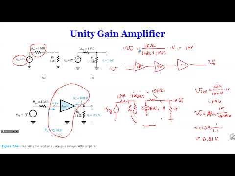
- A unity-gain buffer can raise delivered signal voltage dramatically by isolating a high-resistance source from a low-resistance load, as shown by the 1 V, 1 MΩ source and 1 kΩ load example.
- A MOSFET source follower has ideally infinite input resistance because its gate draws no current, while its output resistance is approximately 1/gm in parallel with the load.
- A BJT emitter follower reflects emitter-side resistance to its base by about β+1, enabling high input resistance without requiring high voltage gain.
- The BJT emitter follower's output resistance is approximately 1/gm when source resistance is excluded, and source resistance contributes roughly Rs/(β+1) when included.
- A near-unity amplifier does not guarantee an output equal to the source voltage: source resistance and input resistance determine the input divider, while output resistance and load determine the output divider.
- A Darlington pair keeps voltage gain near one but can increase input resistance substantially by reflecting the second follower's input resistance through the first transistor.
Chapters
- A 1 V source with 1 MΩ internal resistance driving a 1 kΩ load directly produces only about 1 mV.
- A unity-gain buffer with 100 MΩ input resistance and 100 Ω output resistance can deliver roughly 0.9 V to the same 1 kΩ load.
- The lecture motivates using a near-unity-gain stage between a high-resistance source and a load, even when earlier stages provide the voltage gain.
- In a common-drain MOSFET stage, the drain is at small-signal ground, the gate receives the input, and the output is taken at the source.
- The small-signal T model reduces the gain to approximately RL divided by RL plus 1/gm.
- When RL is much larger than 1/gm, the gain approaches one, giving the circuit its source-follower name.
- MOSFET gate current is approximately zero, so the source follower has very high, ideally infinite, input resistance.
- With the input shorted for the output-resistance test, the output sees approximately 1/gm in parallel with RL.
- Since 1/gm is often much smaller than a kilohm-scale load, the follower can present an output resistance in the tens of ohms.
- The BJT common-collector stage grounds the collector, drives the base through source resistance Rs, and takes its output from the emitter.
- The emitter T-model makes the relationship between base current and emitter current explicit: emitter current is approximately (β+1) times base current.
- The emitter-follower gain approaches one when the source resistance is small relative to the load resistance reflected through the transistor.
- The emitter load is reflected toward the base by roughly a factor of β+1, producing an input resistance of approximately rπ+(β+1)RL.
- For β=100, RL=10 kΩ, and gm=1 mS, the reflected load term alone is about 1.01 MΩ.
- The lecture distinguishes amplifier input resistance from the additional source resistance Rs, which affects the gain from the signal source.
- To find output resistance, short the input signal and apply a test voltage at the emitter output.
- If source resistance is excluded, the output resistance is approximately 1/gm in parallel with RL.
- If Rs is included, its contribution is reduced by the emitter-current gain, giving approximately Rs/(β+1) in series with 1/gm, then in parallel with RL.
- A resistance on the emitter side appears at the base multiplied by approximately β+1.
- A resistance on the base side appears at the emitter divided by approximately β+1.
- The resulting equivalent circuit combines the reflected resistance with 1/gm and RL, making input- and output-resistance estimates more direct.
- The lecture derives gain by reflecting the emitter-side network to the input, then canceling the common small-signal current.
- An alternate output-side voltage-divider calculation gives the same gain, confirming the reflection method.
- Both approaches retain the effects of Rs, 1/gm, β+1, and RL rather than assuming the gain is exactly one.
- A design exercise considers a unity-gain BJT buffer with a stated input-resistance target near 100 kΩ and a 1 kΩ load.
- The lecturer notes that the requested resistance depends on whether RL and the signal source resistance are included in the definition.
- The unknowns include transistor gm and β, so the input-resistance condition alone does not determine a unique design.
- The input-resistance expression includes the reflected emitter network, approximately (β+1)(1/gm+RL), with source resistance treated separately.
- Assuming β=100 and a 100-kΩ target produces very different implications depending on whether the 1-kΩ load is included.
- The example warns that neglecting 1/gm before checking the other given conditions can produce an unreliable estimate.
- The stated output-resistance condition supplies an additional constraint for the design example when source resistance and load are excluded.
- With an output resistance of 10 Ω, the approximation 1/gm≈10 Ω gives gm≈0.1 S.
- Using VT≈25 mV and gm≈IC/VT yields an emitter or collector current of about 2.5 mA.
- Once gm is estimated from the 10-Ω output-resistance condition, the 100-kΩ input-resistance condition can be used to estimate β.
- Including a 1-kΩ emitter load changes the input-resistance calculation substantially compared with excluding it.
- The lecturer flags the example's wording about included resistances as important and recommends checking the stated equivalent-circuit definition.
- The output from the complete source-buffer-load chain includes both the source divider, Rin/(Rs+Rin), and the output divider, RL/(RL+Rout).
- For a 200 mV signal and a source resistance near 100 kΩ driving a 100-kΩ input resistance, the input divider reduces the signal to about 100 mV.
- A near-unity voltage gain cannot compensate for poor source-to-input impedance matching, so the delivered output may be lower than the source voltage.
- A Darlington pair cascades two BJT emitter followers, with the first emitter driving the second transistor's base.
- Because each stage has gain near one, the combined voltage gain also remains near one.
- The second stage's input resistance is reflected through the first transistor by roughly β1+1, greatly increasing the overall input resistance.
- The Darlington pair improves input resistance rather than voltage gain, which remains approximately unity.
- The lecture characterizes its output resistance as similar to that of a single emitter-follower stage under the discussed model.
- The final design choice is between a single follower for basic buffering and a Darlington pair when the source needs a substantially higher input resistance.
Transcript excerpt
0:00 So so far we have covered six types of uh amplifier based on MOSFET and PKTs. So there are three more types that we're going to discuss today. uh will be um well basically there should I should say two more types we have a common drain and common collector but of course when I say there may be there may be a little bit complicated if the resistance um at at one of the terminals that's make a little bit but let's see uh but before I get into the Um before I get into the common and common connect amplifiers, let's look at one example. And why?
0:50 Because the two amplifiers we're going to get to are going to have nearly uh unity amplification or gain. So which means their gains of one. So input and output are almost equal. So one of the big question ask it all the time that why do you need it if it's the gain is only one, right? So we're going to go through this example and you can figure out right away and then we alo have another example to go through show that why the unit gain is impossible. Now the top example shows that we have a power supply and one volt and the power supply comes with a 1 megga of resistance. So apparently I mean this is the common like you have a one volt power sensor I mean input and you have a huge internal resistance and a one Mac is a little bit
1:39 exaggerate but in hundreds of kilohm is is is quite popular. Now this one is um merely to use example saying that it's going to make your life miserable if that is the case when you don't have a unit game. And then on the other hand
This is the start of the transcript. Save this video free for the whole transcript, searchable and time-coded.
In this course
Related notes
Summary, takeaways, and chapters were generated by AI from the video's transcript and may contain errors. The video belongs to its creator, Wireless Power Transfer.