ECircuits-Lec32-2026
Overview
The lecture develops practical small-signal analysis for MOSFET amplifiers, showing how parasitic gate capacitance makes input impedance frequency-dependent and how larger circuits can be analyzed as common-source, common-gate, and common-drain stages. It then introduces PMOS sign conventions and derives MOSFET current mirrors, including the width-ratio rule for scaling currents and the channel-length-modulation limitation.
Key takeaways
- A MOSFET gate has effectively infinite DC input impedance, but parasitic capacitances such as Cgs create AC current paths whose impedance decreases as frequency increases.
- Complex MOSFET amplifiers can often be analyzed by identifying common-source, common-gate, and common-drain stages, then combining their gains and currents.
- In a low-frequency common-gate TIA, an ideal input current source sends its AC current toward the transistor’s approximately 1/gm source impedance when the alternative current-source branch is open.
- For matched MOSFETs with equal channel lengths in saturation, a current mirror scales current according to transistor width: I2/I1 = W2/W1.
- Parallel MOSFETs add effective width, enabling ratios such as 3/2 by using three unit devices on one side and two on the other.
- Channel-length modulation makes a practical current-mirror ratio depend on both device sizing and drain voltages, through the factor (1 + λVDS2)/(1 + λVDS1).
Chapters
- The November 6 lecture will be held on Zoom, and Homework 6 is due November 9.
- A MOSFET gate blocks DC current through its silicon dioxide insulator, but parasitic capacitances such as Cgs provide AC current paths.
- As frequency rises, capacitive impedance falls, so the MOSFET input impedance is not infinite in the AC small-signal model.
- Common-source amplifiers invert the signal, producing a 180-degree phase shift because drain current and the measured drain-load voltage have opposite signs.
- Common-gate and common-drain stages are non-inverting; the source follower has voltage gain near one.
- Recognizing the input, output, and common terminals identifies the stage type inside a more complex circuit.
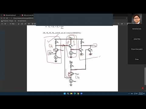
- The Homework 6 circuit can be divided into a common-gate input stage, a source follower, another common-gate stage, and common-source output stages.
- The output voltage is generated by the combined currents from two common-source transistors flowing through the shared output resistance.
- Because the input is current and the output is voltage, the overall transfer quantity is transimpedance, measured in ohms.
- In the worked example, an ideal current source injects the entire small-signal input current into the common-gate stage because its downward path has infinite impedance.
- The common-gate input presents approximately 1/gm, while the drain load R1 converts the input current into a voltage: Vout1 = Iin × R1.
- That voltage drives two common-source transistors; their output currents add by KCL, and the sum flows through R2.
- With equal gm values, infinite ro, and R1 and R2 each equal to 1/gm, the simplified transimpedance is proportional to 1/gm.
- For small-signal analysis, DC current sources are opened and DC voltage sources are shorted to AC ground.
- Unlike the simpler example, the Homework 6 input node has a path through a MOSFET source with impedance approximately 1/gm3.
- The input current therefore sees R1 in parallel with 1/gm3, and that equivalent resistance determines the node voltage.
- The MOSFET gate path remains effectively open because parasitic capacitances are excluded in this low-frequency problem.
- A PMOS is the polarity dual of an NMOS: its threshold voltage is negative, and it turns on when VGS is more negative than VT.
- A negative gate voltage attracts positively charged holes to form the PMOS channel between its P-type source and drain regions.
- Using absolute values for threshold voltage, overdrive, and terminal voltages makes many NMOS and PMOS equations take the same form.
- MOSFET symbols vary across books and tools; the LTspice symbol marks the source terminal, so source and drain cannot simply be interchanged in the model.
- In a physical MOSFET, terminal roles depend on bias: the higher-potential terminal is the NMOS drain, while the higher-potential terminal is the PMOS source.
- For an NMOS example with VT = 0.7 V and Vov = 0.3 V, VGS = 1 V; saturation requires VDS to exceed 0.3 V.
- For a PMOS with source at 5 V and gate at 4 V, VGS = -1 V; saturation is checked using absolute terminal voltage and overdrive.
- Previously covered blocks include common-source, common-gate, and common-drain amplifiers, plus MOSFETs used as resistances.
- Looking into a MOSFET source or a diode-connected drain gives approximately 1/gm; looking into a non-diode-connected drain gives ro.
- A current mirror copies a reference current into other circuit branches, avoiding the need for a separate external current source for every amplifier stage.
- Current mirrors provide bias currents for analog IC blocks and will be used in the upcoming differential-amplifier discussion.
- The reference transistor M1 is diode-connected, and M1 and M2 share gate and source connections, so their VGS values and, for matched devices, overdrive voltages are equal.
- If M2 remains in saturation, the ideal square-law equations give I2/I1 = K2/K1.
- Since K = K′W/L and the devices share the same process, equal channel lengths yield I2/I1 = W2/W1.
- Choosing a 2:1 width ratio produces twice the reference current, while equal widths produce a 1:1 current copy.
- Parallel equal-width MOSFETs act like a single device with their widths added: two devices form an effective 2W width, and three form 3W.
- A mirror with two equal-width devices on the reference side and three on the output side produces I2 = 3/2 × I1, assuming matched devices and equal lengths.
- Channel-length modulation changes the ideal ratio by the factor (1 + λVDS2)/(1 + λVDS1), so unequal drain voltages introduce mirror error.
- The course analysis neglects λ, but more advanced analog IC design must account for this nonideality.
Transcript excerpt
0:07 All right. So, uh Just a quick announcement that November 6th, that is the Friday, I'm I'll be traveling and so the lecture will be on Zoom. Uh no need to come to the class here because I'll not be here, but if you want to attend the lecture from here, please feel free to do so. I'll be teaching the class over Zoom. Um homework four and five you guys have already submitted. Make sure you also submit your homework number six. That will be due on November 9th. And related to that we'll be discussing a few um important concepts in today's lecture. So, for example, the first question that you see for homework number six is an amplifier where the input is provided at the gate.
0:55 Uh the small signal input impedance is what is asked in this question. So, what is your Z in looking at the input terminal? Now, of course, for a MOSFET, you know that looking at the input terminal, you're going to see infinite impedance because the MOSFET input has a um insulator, that is the silicon dioxide material, and no current no DC current can pass through the silicon dioxide because it's an insulator, right? It cannot It does not allow current to pass through. However, interestingly, there is always some amount of capacitance between your gate and the source node. There is some amount of capacitance between your drain and the source node. There is always some amount of capacitance between the gate and the source nodes, and so on, right? Now, if that is true Now Now that is true for for any physical
1:44 material, right? Whenever you have a physical geometry, uh you have a physical device, you have two nodes, there is always electrical coupling between them. Even as I I I
This is the start of the transcript. Save this video free for the whole transcript, searchable and time-coded.
In this course
Related notes
Summary, takeaways, and chapters were generated by AI from the video's transcript and may contain errors. The video belongs to its creator, WISE Lab - UF ECE.