ECircuits-Lec35-2026
Overview
The lecture develops MOS differential amplifiers from their differential and common-mode behavior through diode-connected, current-source, and current-mirror loads, deriving how each load affects gain and output structure. It then connects these stages to op-amp design: common-mode feedback controls output bias, cascaded gain stages raise amplification, a source follower lowers output impedance, and frequency compensation is still needed to achieve a single dominant pole.
Key takeaways
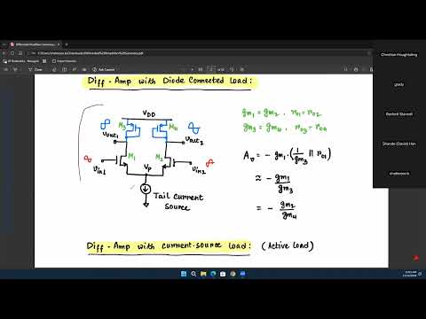
- A diode-connected PMOS load presents approximately 1/gm at the output, so the differential-stage gain is constrained by the input-to-load transconductance ratio.
- A saturated current-source load increases gain by replacing the diode load resistance with ro, making output resistance approximately ro of the NMOS in parallel with ro of the PMOS.
- Common-mode feedback regulates the average of the two output DC voltages against a target such as VDD/2, adjusting PMOS bias to stabilize output levels and branch currents.
- A current-mirror load combines branch currents so a single-ended output is proportional to Vin1 minus Vin2, with gain approximately minus gm(ro2 parallel ro4).
- Cascaded gain stages can raise open-loop gain, while a source follower with output resistance near 1/gm provides the low-impedance output drive an op-amp needs.
- High gain and low output impedance are not sufficient for a practical op-amp: parasitic RC networks create multiple poles, so frequency compensation must establish a single dominant pole and a minus 20 dB per decade roll-off.
Chapters
- Lab 7 covers CMOS logic circuits and transmission gates, and is due the following week.
- Homework 8 on logic circuits and transmission gates is due November 30, after Thanksgiving.
- The upcoming op-amp design example leads into Homework 9, due in the first week of December.
- Define the differential input as Vin1 minus Vin2 and the differential output as Vout1 minus Vout2.
- For differential-mode operation, the two inputs are equal-amplitude signals 180 degrees out of phase; the shared source node VP acts as a virtual ground.
- Common-mode rejection ratio is differential-mode gain divided by common-mode gain; transistor mismatch and other nonidealities create a nonzero common-mode output.
- Under symmetric half-circuit analysis, a common-source differential stage has gain approximately minus gm times the parallel combination of RD and ro.
- With a diode-connected PMOS load M3, the small-signal resistance looking into its drain is approximately 1/gm3.
- The input NMOS drain contributes ro1, giving a stage gain approximately minus gm1 times (ro1 parallel 1/gm3).
- When the diode-connected load conductance dominates, gain is roughly the ratio gm1/gm3; designers can adjust transistor W/L ratios to change transconductance.
- Use the MOSFET small-signal equivalent circuit and a test source to derive node resistance when a familiar result such as 1/gm is uncertain.
- Biasing the PMOS load in saturation makes the output resistance approximately ro1 parallel ro3, so gain becomes about gm1(ro1 parallel ro3).
- The load transistors and tail source all constrain branch currents; mismatched independent current sources can fight and shift the operating point.
- Common-mode feedback low-pass filters the two output voltages, compares their average with a target such as VDD/2, and uses the error amplifier output as the PMOS bias VBP.
- The feedback adjusts VBP and PMOS VSG to correct output common-mode voltage, controlling device VDS and reducing current errors associated with channel-length modulation.
- A PMOS current mirror copies the small-signal branch current from one side of the differential pair into the other.
- Taking the output at a single mirrored-branch node produces a single-ended signal proportional to Vin1 minus Vin2.
- The output resistance is approximately ro2 parallel ro4, giving voltage gain about minus gm1(ro2 parallel ro4).
- Unlike a differential-output stage with current-source loads, the current-mirror load performs differential-to-single-ended conversion.
- To find the effective transconductance, AC-ground the output and divide the resulting output current by the differential input voltage.
- The M1 branch contributes gm1Vin1 and the M2 branch contributes gm2Vin2; the mirror combines these currents with opposite signs.
- For matched input transistors, the net output current is gm(Vin1 minus Vin2), demonstrating inherent differential subtraction.
- Multiplying this effective transconductance by ro2 parallel ro4 gives the single-ended voltage gain.
- MOS gate inputs provide ideally infinite input impedance, and transistor sizing can make the differential stage gain large.
- The current-mirror stage output impedance, ro2 parallel ro4, is large rather than the near-zero output impedance required of an op-amp.
- Cascading stages can increase gain; for example, two stages with gain 20 each produce an overall gain of about 400.
- A source follower provides near-unity voltage gain, gmRs/(1 + gmRs), and output resistance approximately 1/gm, which can be made small by increasing gm.
- A usable op-amp also needs suitable frequency behavior, not just high gain, high input impedance, and low output impedance.
- The target is a single dominant pole, producing a minus 20 dB per decade gain slope beyond the bandwidth.
- Additional poles from parasitic resistances and capacitances at successive amplifier stages can steepen roll-off to minus 40 dB per decade or more.
- The next op-amp design work addresses how to control the poles; the next class first detours to CMOS logic and transmission gates for Lab 7 and Homework 8.
Transcript excerpt
0:01 Okay, so we are towards the very end of the semester and for this course as well. We have about five or six lectures remaining. Today's lecture 35 and we had been discussing about differential amplifiers over the last few lectures. So today we'll summarize the differential amplifiers and look at how these differential amplifier topology can eventually lead to an op-amp topology. So you eventually learn about how to design an op-amp towards the end of the class. There is one other topic that is still remaining is about CMOS logic circuits and transmission gates which also actually forms your lab seven. So lab seven is due next week. We would like to wrap up with all the labs before Thanksgiving. So lab seven talks about
0:48 CMOS logic circuits and transmission gates. Because we haven't yet started discussing about CMOS logic and T gates, I have uploaded a video from previous year. So please take a look at it before you go for the lab on Monday, for example. But I'm planning to cover, if time permits, a little bit of that towards the later part of today's class as well as on Monday so that you are prepared with the contents of lab seven, so which contains CMOS logic circuits and transmission gates. Homework eight will be on logic circuits and T gates, which will be due after Thanksgiving, November 30th. And in the meantime, next week we will also learn about how to design an op-amp from all the concepts that we have learned throughout the semester. So that op-amp design example is something that
1:35 we'll cover next week. And homework nine, which will be on an op-amp design, would be would be due in the first week of December. So that's that's about it for the
This is the start of the transcript. Save this video free for the whole transcript, searchable and time-coded.
In this course
Related notes
Summary, takeaways, and chapters were generated by AI from the video's transcript and may contain errors. The video belongs to its creator, WISE Lab - UF ECE.