ECircuits-Lec37-2026
Overview
The lecture connects CMOS logic design to transistor behavior and timing: derive an NMOS pull-down network from the output-zero condition, make the PMOS pull-up its dual, and account for switching activity and RC delay. It analyzes why transmission gates combine NMOS and PMOS switches, applies resistance and timing estimates to logic examples, then reviews multistage op-amp architecture and why pole splitting is needed for stable, single-pole-like behavior.
Key takeaways
- For static CMOS logic, derive the NMOS pull-down network from the condition that the output is zero, then form the PMOS pull-up network by swapping series and parallel connections.
- Dynamic power scales as αCV²f: reducing switching activity, load capacitance, supply voltage, or clock frequency reduces power consumption.
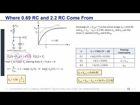
- An RC output reaches 50% of its final value in about 0.69RC and traverses the 10% to 90% range in about 2.2RC, linking gate resistance and load capacitance directly to speed.
- NMOS switches pass zero strongly but degrade near a logic one, while PMOS switches pass one strongly but degrade near zero; a complementary transmission gate combines their strengths.
- In a CMOS logic gate, PMOS pull-up devices charge the output toward VDD and NMOS pull-down devices discharge it toward ground, avoiding the threshold-limited levels that result when their roles are reversed.
- Multistage op amps accumulate RC poles at internal nodes; pole splitting separates those poles to improve the amplifier's frequency response and approximate single-pole behavior.
Chapters
- Start with the Boolean equation or derive it from a truth table, then identify when the output is zero to construct the NMOS pull-down network.
- Translate AND operations into series transistor connections and OR operations into parallel connections in the pull-down network.
- Create the PMOS pull-up network as the dual: replace series connections with parallel ones and vice versa.
- Charging a load capacitor draws CV² from the supply, stores ½CV², and dissipates the other ½CV²; discharging dissipates the stored energy.
- A complete charge-discharge cycle consumes CV², giving dynamic power P = αCV²f when switching activity is included.
- The activity factor α ranges from 0 for a circuit that never switches to 1 for one that switches every clock cycle.
- A gate must charge or discharge its output within a small fraction of the clock period for the next stage to recognize a valid logic level.
- For an RC load, the 50% propagation delay is approximately 0.69RC for both rising and falling transitions.
- The 10% to 90% rise time, or 90% to 10% fall time, is approximately 2.2RC.
- The capacitor charging curve is Vout = VDD(1 − e^(−t/RC)); defining x = Vout/VDD gives tx = RC ln(1/(1 − x)).
- At x = 0.5, the output reaches half its final voltage after 0.69RC, the propagation-delay convention used in the lecture.
- The time difference between reaching 10% and 90% is RC ln(9), approximately 2.2RC, a value applied to Homework 8.
- A transmission gate places an NMOS and a PMOS in parallel between input and output, using a control signal and its complement.
- The NMOS turns on with a logic-high gate control, while the PMOS turns on with a logic-low gate control, so both conduct together.
- The combined switch passes the input when enabled and is also called a pass gate.
- In the triode region, the NMOS conductance depends on gate overdrive and drain-source voltage; its on-resistance increases as the passed input voltage rises.
- With the gate at VDD, the NMOS becomes weak near an input of VDD − VTN, so it cannot pass a strong logic one.
- An NMOS switch is therefore effective at passing a logic zero but poor at passing a logic one.
- The PMOS has the complementary pass behavior: it passes a strong logic one well but performs poorly when passing a logic zero.
- Putting NMOS and PMOS on-resistances in parallel keeps the transmission gate's effective resistance lower than either device alone across the input range.
- This same pass-strength difference motivates using PMOS devices for CMOS pull-up paths and NMOS devices for pull-down paths.
- A pull-up network made from PMOS devices can charge the output to VDD, while an NMOS pull-down network can discharge it to ground.
- Reversing those device roles causes degraded logic levels: an NMOS pull-up may stop near VDD − VT, and a PMOS pull-down may stop near |VT|.
- For the discussed Boolean example, the NMOS network uses parallel A and B branches, a series C connection, and a parallel D path; the PMOS network is its dual.
- The Homework 8 example uses VDD = 5 V, NMOS and PMOS threshold values of 0.7 V and 0.6 V, and device parameters KN = 5 and KP = 3, with λ = 0.
- The example estimates on-resistances of about 46 Ω for an NMOS and 75 Ω for a PMOS; the active transistor paths change with the input combination.
- For one discharge case, 46 Ω in parallel with 46 Ω + 46 Ω gives 31 Ω; with a 10 pF load, the 50% delay is about 214 ps.
- The worst-case path is the one with the largest effective resistance; the lecture identifies a 225 Ω example and notes that larger RC means a lower maximum operating frequency.
- A differential input stage with current-source loads can provide high input impedance and gain; common-mode feedback helps prevent current sources from fighting each other.
- A current-mirror-loaded differential amplifier provides a single-ended output, while a source follower can serve as the final stage.
- The source follower has output resistance near 1/gm, and transistor-gate inputs offer high impedance, though parasitic capacitances matter at high frequencies.
- Parasitic capacitance at each resistive circuit node creates an RC pole, so a multistage amplifier naturally has multiple poles.
- A single-pole response falls at −20 dB per decade after its pole; additional poles steepen the slope to −40 dB per decade or more.
- For a single-pole op amp, gain-bandwidth product matches unity-gain frequency; with multiple poles, unity-gain crossover differs.
- The next design topic is pole splitting, which separates poles to make a multistage op amp behave more like a single-pole system.
Transcript excerpt
0:04 All right. So your homework eight basically deals with different kinds of logic circuits. Um even in your lab seven you're dealing with these logic circuits and how do you implement different types of logic circuits with SMOS. Um as we discussed in the last lecture the way you design any kind of logic circuit is to first look at the equation. You can go with the truth table based approach as we had discussed in the last lecture. But an even easier approach is that from the truth table if you are able to find out the equation let's say the equation is not given and only the truth table is given. You can find out the equation uh just from the truth table. Now once you have the equation then the easiest way to implement it is think about how this output can get discharged because the discharge path
0:52 will be happening through this pull down network which is implemented using INOS whereas the pull up network which pulls up the output to VDD that gets implemented using POS. So this is pull up that gets implemented using POS and this is pull down network that is imple network that gets implemented with N MOS right so the easiest way to implement this is that look at the equation and implement the discharge path that is what does the pull down network do that discharges the output to ground now the equation always gives you when is the output equal to one when is the output equal to one that is given in the equation what you're looking at in The pull down network is when is the output zero. So when is the output getting zero? For that you will implement if
1:40 your V out is equal to let's say any
This is the start of the transcript. Save this video free for the whole transcript, searchable and time-coded.
In this course
Related notes
Summary, takeaways, and chapters were generated by AI from the video's transcript and may contain errors. The video belongs to its creator, WISE Lab - UF ECE.