ECircuits-Lec16-2026
Overview
The lecture develops a circuit-level model of PN diodes, connecting carrier movement and depletion-region changes to the diode equation, leakage, threshold voltage, and resistance. It then applies practical silicon-diode models to circuit calculations and load-line analysis, including a 10 V example with a 330 ohm resistor and two matching diodes.
Key takeaways
- Reverse bias widens a PN diode's depletion region and suppresses majority-carrier flow, while forward bias narrows it and enables substantial current.
- The Shockley model I_D = I_S(exp(V_D/(nV_T)) - 1) explains zero current at zero bias, reverse current approaching -I_S, and exponential forward-current growth.
- At about 300 K, silicon's thermal voltage is roughly 25.8 mV, so a forward-biased diode's small-signal resistance is approximately n × 25.8 mV divided by its DC current.
- Common approximate diode drops are 0.3 V for germanium, 0.7 V for silicon, and 1.1 to 1.2 V for gallium arsenide, though operating conditions affect the actual values.
- A 10 V supply, 330 ohm resistor, and 0.7 V diode drop produce about 28 mA; two identical parallel diodes share that current at about 14 mA each.
- A load-line intersection between the diode I-V curve and the source-resistor constraint identifies the operating point and shows how changing resistance shifts the diode current and voltage.
Chapters
- Lab 3 receives two weeks so students can finish it, catch up on Labs 1 or 2, and avoid overlapping exam and lab deadlines.
- Students who finish Lab 3 during the current week do not need to attend the following week's lab session.
- Lab 4 will not begin until Lab 3 is finished, so the two labs will not overlap.
- An optional self-study resource covers diode behavior from a device-physics perspective, beyond the circuit-level treatment in ECE 3308.
- Students are asked to review the uploaded BJT introduction and basics before upcoming lectures on bipolar junction transistors.
- The next two lectures are expected to introduce and develop BJT analysis.
- Boron-doped silicon forms P-type material with holes as majority carriers; phosphorus- or arsenic-doped silicon forms N-type material with electrons as majority carriers.
- In reverse bias, the battery pulls majority carriers away from the junction, widening the depletion region and strongly suppressing current.
- In forward bias, the battery pushes holes and electrons toward the junction, narrowing the depletion region and enabling carrier flow.
- Holes move in the direction of conventional current, while electrons move in the opposite direction; ionized dopants remain immobile.
- Even with no applied voltage, electron-hole recombination near the PN junction creates a depletion region.
- A small forward voltage produces little current until the depletion region is sufficiently reduced, after which forward current rises steeply.
- Reverse current is small but nonzero because minority carriers, such as holes in N-type material and electrons in P-type material, can contribute to current.
- The real diode therefore differs from an ideal diode, which is an open circuit in reverse bias and turns on at zero forward voltage.
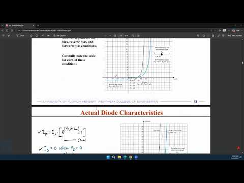
- The diode current is modeled as I_D = I_S(exp(V_D/(nV_T)) - 1), where I_S is reverse saturation current, V_D is diode voltage, V_T is thermal voltage, and n is the nonideality factor.
- At V_D = 0, the exponential term makes I_D zero; at sufficiently negative V_D, current approaches -I_S, the reverse leakage level.
- For forward bias, the exponential term dominates and predicts the rapid current increase beyond the turn-on region.
- At room temperature near 300 K, V_T = kT/q is about 25.8 mV; the silicon nonideality factor n is commonly taken as approximately 1 to 1.3.
- Typical approximate turn-on voltages are 0.3 V for germanium, 0.7 V for silicon, and 1.1 to 1.2 V for gallium arsenide diodes.
- Actual forward voltage depends on factors including semiconductor technology, doping, temperature, and operating conditions.
- Static DC resistance at an operating point is V_D/I_D, following Ohm's law.
- Circuit analysis distinguishes static resistance, small-signal AC resistance, and average AC resistance.
- A diode is first biased at a DC operating point; a small AC voltage around that point creates a corresponding current variation.
- Dynamic resistance is the local ratio of voltage change to current change, r_d = dV_D/dI_D, rather than the DC ratio V_D/I_D.
- Differentiating the forward Shockley relation gives r_d approximately nV_T/I_D; with n near 1 at room temperature, this is about 26 mV divided by the bias current.
- Reverse-biased diodes have very high dynamic resistance because their current is near zero, while forward-biased diodes have lower dynamic resistance as current increases.
- Average AC resistance uses the finite ratio ΔV_D/ΔI_D between two points; the small-signal value is the limiting derivative as the interval approaches zero.
- A practical diode model represents a silicon turn-on threshold with a 0.7 V source in series with diode resistance and an ideal diode.
- Use DC resistance for DC analysis and small-signal dynamic resistance for AC analysis around a bias point.
- The model makes the diode's threshold and nonzero resistance explicit instead of treating the real device as an ideal short or open.
- For basic circuit calculations, the piecewise approximation treats a silicon diode as off below about 0.7 V and as conducting with roughly a 0.7 V drop when forward biased.
- With a 10 V supply and a 330 ohm resistor, the resistor drops 9.3 V when the diode drop is 0.7 V, giving approximately 28 mA.
- If that current feeds two identical parallel silicon diodes, it divides approximately equally, or about 14 mA per diode.
- The diode's internal resistance can be neglected when it is unspecified and much smaller than the 330 ohm circuit resistance, but a provided resistance must be included.
- The diode's I-V curve is combined with the resistor-and-source load line; their intersection gives the circuit's operating point, or Q point.
- For a source E and series resistance R, the load-line endpoints are I_D = E/R when V_D = 0 and V_D = E when I_D = 0.
- Changing R changes the load-line slope and intersection, while the diode's characteristic remains the same.
- Using the measured diode I-V curve can give a more accurate graphical solution than assuming an abrupt 0.7 V turn-on; rectifier applications are introduced as the next topic.
Transcript excerpt
0:02 All right. So, uh first off, I think some of you guys have asked uh questions on the timelines of lab 3. Uh this is to note that lab three will be for two weeks and this is just the timeline for lab three. It does not um there were some questions that okay can you start lab four on that week but because lab four has not been posted you cannot start lab four in the next week. Um so lab three we're giving two weeks for everyone to complete lab three as well as if you are if you want to let's say catch up with some of the contents of lab two or lab one if someone has missed lab two or lab one this would be a good time to catch up so that is the only reason lab three is for two weeks uh and of course because we have the exam due this week as well as um lab three uh being due next week so I just wanted to
0:51 scatter the deadlines a little bit and that is the main reason why Lab three has been extended for two weeks. >> Uh yes, question. >> So we can go to lab this week. Our lab section done in time. >> Um yeah. So if you if you're done with lab three this week, you don't need to go next week. >> Okay. Right. So we can do your lab time. >> Yes. >> Yes. >> Yes. Question. like lab session or lab won't start till after everyone >> until lab three is finished. So there will be no overlapping lab three and lab four until and unless lab three is finished will not start in lab four. All right. And uh in terms of the
This is the start of the transcript. Save this video free for the whole transcript, searchable and time-coded.
In this course
Related notes
Summary, takeaways, and chapters were generated by AI from the video's transcript and may contain errors. The video belongs to its creator, WISE Lab - UF ECE.