ECircuits-Lec34-2026
Overview
The lecture develops small-signal analysis of a MOSFET differential pair, moving from superposition and half-circuit methods to differential-mode and common-mode behavior. It derives the ideal differential gain of approximately -gmRD, explains how device mismatch limits common-mode rejection ratio (CMRR), and shows how source degeneration trades gain for a wider linear input range.
Key takeaways
- An ideal tail-current source makes differential-pair bias current less sensitive to input gate voltage, helping stabilize transistor overdrive voltage and gm.
- For a symmetric MOSFET differential pair under equal-amplitude, 180-degree differential excitation, the shared source node is an AC virtual ground and each half reduces to a common-source amplifier.
- The ideal differential gain is approximately -gmRD, or -gm(RD parallel ro) when transistor output resistance is included.
- An ideal differential pair has zero common-mode gain and infinite CMRR, but transistor and load mismatch convert common-mode input into differential output and make real CMRR finite.
- Source degeneration reduces gain through the factor 1 + gmRS while extending the linear input range; when gmRS is large, gain approaches -RD/RS and becomes less sensitive to gm variation.
Chapters
- A tail current source biases the differential-pair transistors by current, helping keep their drain currents, overdrive voltages, and gm stable as gate DC voltage changes.
- Ideally, matched transistors M1 and M2 and matched loads RD1 and RD2 produce zero input offset; mismatch can create an op-amp input offset.
- The MOSFET small-signal model uses a dependent current source gmVGS between drain and source, with ro added to model channel-length modulation.
- Differential voltage gain is the AC differential output, Vout1 minus Vout2, divided by the AC differential input, Vin1 minus Vin2.
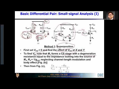
- With Vin2 set to AC ground, M1 acts as a common-source stage whose source sees an effective degeneration resistance looking into M2.
- For large ro2, the resistance looking into M2's source is approximately 1/gm2; with finite ro2, it depends on ro2, RD2, and the factor 1 + gm2ro2.
- The M1-to-node-x gain is approximately -gm1RD1/(1 + gm1RS), where RS is the effective resistance at the shared source node.
- The analysis treats DC supplies as AC ground and an ideal DC tail-current source as an open circuit.
- To find the response at node y from Vin1, the M1 source-follower path is replaced by a Thevenin equivalent with approximately 1/gm1 output resistance.
- M2 then operates as a common-gate stage, giving a positive-phase response of approximately RD/(1/gm1 + 1/gm2), unlike the inverting common-source response at node x.
- Superposition combines the node-x and node-y contributions from each input; for matched gm values and loads, the differential output gain reduces to approximately -gmRD.
- Including transistor output resistance replaces RD with RD in parallel with ro in the common-source gain approximation.
- For a symmetric differential pair driven by equal-amplitude inputs 180 degrees out of phase, the two source-follower responses cancel at the shared source node.
- The shared source node is therefore an AC virtual ground, although it retains a nonzero DC voltage required to keep the tail current source operating properly.
- Each half of the differential pair becomes a common-source amplifier, so its gain is approximately -gmRD, or -gm(RD parallel ro) when ro is included.
- Half-circuit analysis requires symmetry in both branches and complementary differential excitation; unequal amplitudes, phase errors, or component mismatch invalidate the simplification.
- Any two input signals V1 and V2 can be decomposed into a common-mode component (V1 + V2)/2 and equal-and-opposite differential components of magnitude (V1 - V2)/2.
- The decomposition works even when the original inputs do not have equal amplitudes or a 180-degree phase difference.
- Analyzing the differential component separately gives a differential output proportional to -gm(RD parallel ro)(V1 - V2).
- The common-mode component must be analyzed separately because its behavior is distinct from the differential-mode response.
- With perfectly matched branches and an ideal tail-current source, equal common-mode inputs do not change the differential output; the ideal common-mode gain is zero.
- Differential-mode gain is approximately -gmRD, while common-mode rejection ratio is the magnitude of differential gain divided by common-mode gain.
- Ideal CMRR is infinite because the ideal common-mode gain is zero; real transistor and resistor mismatch converts some common-mode input into differential output.
- A real differential amplifier therefore has finite CMRR, often expressed in decibels as 20 log10 of the differential-to-common-mode gain ratio.
- Matched source resistors RS1 and RS2 preserve the AC virtual-ground condition for differential excitation, allowing each branch to be analyzed as a degenerated common-source stage.
- Source degeneration lowers gain according to approximately -gmRD/(1 + gmRS), but extends the input range over which the response remains linear.
- Without degeneration, gain depends directly on gm, which changes as the differential input moves away from its balanced operating point.
- When gmRS is much greater than 1, the gain approaches -RD/RS, reducing sensitivity to process-dependent gm variation.
- Differential-pair resistive loads can be replaced with MOSFET loads, including diode-connected devices M3 and M4 or transistor current-source loads.
- With diode-connected loads, a branch gain can be approximated by the ratio of input-device gm to load-device gm; with current-source loads, gain depends on the input gm and the parallel output resistances.
- The lecture flags detailed common-mode response and mismatch equations as advanced material beyond the core course coverage.
- The closing review reiterates that differential gain follows the common-source half-circuit result and previews differential pairs with active loads and their use in op-amp design.
Transcript excerpt
0:11 All right. So we had been discussing differential amplifiers and we started these discussions in the previous lecture which was over zoom. So please make sure you go over that lecture if you have not done that already. So in the last lecture we looked into the large signal analysis of um uh the basic differential pair. Um we looked into why this tail current source is required over here and what does it do? Basically it makes sure that your transistors are biased using a current and not using the VGS voltage. Now in most cases you would see that any analog circuit will generally um so zoom is creating a little bit of
1:04 problem today. Um I hope everybody on zoom is able to hear. Uh if not let me know. But uh what we discussed in the last lecture is that you have this current source over here which makes sure that your transistors are biased using a current and not using a voltage. Because if your transistor over here M1 is biased using a voltage VGS then of course um if you if your DC voltage at the gate goes up or goes down your VGS will change. And because your VGS is going to change, your currents will change, your GM will change. If your GM changes, your gain changes and everything goes haywire. So instead of biasing the transistors using voltages, you generally bias transistors using currents. The advantage there is that for example in
1:52 this circuit as you're biasing the transistors using this current you know that the equation for your V over is going to be square root of ID or whatever current is flowing through those transistors divided by K and that current is a fixed quantity K is a fixed
This is the start of the transcript. Save this video free for the whole transcript, searchable and time-coded.
In this course
Related notes
Summary, takeaways, and chapters were generated by AI from the video's transcript and may contain errors. The video belongs to its creator, WISE Lab - UF ECE.