ECircuits-Lec31-2026
 Watch on YouTube →
Overview
The lecture completes a MOSFET small-signal analysis reference by relating system gain to effective transconductance and output resistance, then applies resistance-looking-in results to source followers, common-gate stages, and diode-connected devices. It compares PMOS diode-connected loads and saturation-biased current-source loads, including example gains of about -5 and -13.4, then derives how a cascode combines common-source and common-gate action to raise output resistance and gain while limiting output swing.
Key takeaways
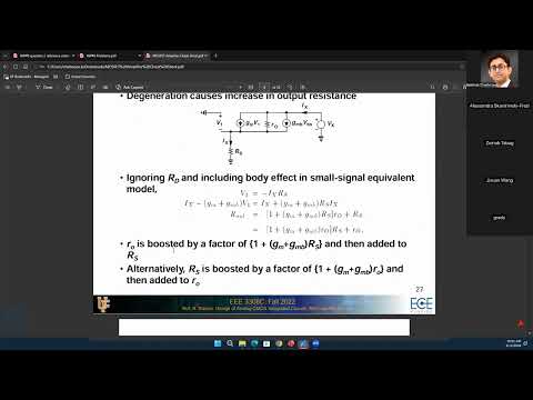
- For a MOSFET with source degeneration, the drain-looking resistance is r_o + (1 + g_mr_o)R_S, so even a modest source resistance can greatly increase output resistance and potential gain.
- A source follower is useful as a buffer rather than a voltage-gain stage: its gain approaches 1 while its output resistance can be reduced to roughly 1/g_m.
- A diode-connected MOSFET presents approximately 1/g_m at its drain and is guaranteed to remain in saturation when on, making it a compact but relatively low-resistance active load.
- Replacing a diode-connected load with a saturation-biased current-source load changes the output load from roughly 1/g_m to r_o, raising the example gain from about -5 to -13.4.
- A cascode uses the common-gate transistor to multiply the resistance seen at the common-source transistor's drain, increasing gain while requiring extra bias headroom and reducing output swing.
Chapters
- The lecture continues a MOSFET AC-analysis summary and previews PMOS circuits, current mirrors, and future differential-amplifier topics.
- Lab 6 runs from November 2 to November 12; Wednesday lab sections should complete it before the following Wednesday holiday.
- Lab 7 is scheduled for the week after, with all labs intended to finish before Thanksgiving.
- The November 6 class is online over Zoom because of conference travel.
- The small-signal system gain is the effective transconductance multiplied by the effective output resistance.
- Find effective transconductance by shorting the load and taking output current divided by input voltage; find unloaded output resistance looking into the output node.
- Looking into a MOSFET drain without source resistance gives approximately r_o.
- With source resistance R_S, drain resistance becomes r_o + (1 + g_m r_o)R_S; for r_o = 100 kΩ, R_S = 10 kΩ, and g_m r_o = 20, it is 310 kΩ.
- A common-drain source follower takes input at the gate and output at the source, with gain g_mR_S/(1 + g_mR_S), approaching but not reaching 1.
- Its output resistance is approximately 1/g_m in parallel with the source resistance, so increasing g_m makes it a stronger load driver.
- A 1 kΩ source resistance driving a 50 Ω load directly gives a voltage divider ratio of 1/21.
- With g_m = 20 mS, 1/g_m is 50 Ω; with g_m = 200 mS, it is 5 Ω, allowing a source follower to drive a 50 Ω load effectively.
- Looking into the source with an unloaded drain gives approximately 1/g_m when r_o is large.
- With a drain resistance R_D, the source-looking resistance is (r_o + R_D)/(1 + g_mr_o), demonstrating a resistance-division effect.
- The common-gate stage grounds the gate, takes input at the source, and takes output at the drain.
- Common-gate gain has the opposite sign from common-source gain, so its input and output are in phase rather than separated by 180 degrees.
- A diode-connected MOSFET ties gate to drain; looking into either terminal gives approximately 1/g_m, unlike the usual drain resistance r_o.
- Applying a test voltage gives i_x = g_mV_x + V_x/r_o, so the resistance is r_o/(1 + g_mr_o), approximately 1/g_m.
- Because V_DS = V_GS, the diode-connected NMOS is always in saturation when on.
- Reversing the applied polarity swaps the MOSFET's source and drain roles, makes V_GS zero, and turns the device off, giving diode-like one-way conduction.
- A PMOS diode-connected load can replace a physical drain resistor, which can consume substantial silicon area.
- The PMOS load contributes approximately 1/g_m2 looking into its drain; the NMOS amplifier contributes r_o1 at the output.
- The common-source gain is approximately -g_m1(r_o1 || 1/g_m2), which reduces to about -g_m1/g_m2 when 1/g_m2 dominates.
- Using g_m = √(2K I_D) and equal branch currents gives a gain magnitude near √(K_1/K_2); with equal channel lengths and electron mobility about twice hole mobility, it depends on the square-root width ratio.
- A PMOS load biased in saturation behaves as a current source, replacing the diode-connected load's approximately 1/g_m resistance with its larger r_o.
- The amplifier output resistance becomes r_o1 || r_o2, increasing gain compared with a diode-connected load.
- For g_m1 = 200 μS, g_m2 = 40 μS, r_o1 = 100 kΩ, and r_o2 = 200 kΩ, the diode-load gain is about -5.
- The same values give a current-source-load gain of about -13.4; unlike the diode-connected case, the designer must bias the load transistor to keep it in saturation.
- A cascode combines a common-source input transistor with a common-gate transistor above it, with both devices biased in saturation.
- The common-gate device makes the resistance looking down from the output approximately r_o2 + (1 + g_m2r_o2)r_o1.
- With a sufficiently large upper load resistance, the common-source and common-gate gains combine, producing a gain proportional to g_m1r_o1 times g_m2r_o2.
- Adding cascode devices can raise gain further, but adds biasing complexity and reduces output swing; folded cascodes are mentioned as an alternative.
Transcript excerpt
0:06 Okay. So, uh today we'll be continuing our discussions on the MOSFET AC analysis. And uh last class we started discussing about a cheat sheet or basically a summary table of all the different kind of circuits we have seen for MOSFET AC or small signal analysis. We'll complete that. We'll also take a look at uh how do we analyze POS based circuits because till now what we have looked into is just NOS. So we look into POS as well as current meters which is another a circuit construct that we'll be learning about today and from next lecture onwards we'll be looking into differential amplifiers uh and the applications of differential amplifiers. We'll look into that in details and what is the difference between what we have seen till now with differential amplifiers.
0:53 Uh a note on the Friday's lecture. Uh this week's Friday, November 6. Uh I'll be teaching this lecture on Zoom because I'll be traveling for a conference during this time. So uh Friday, no need to come into the class. You may come into the class, but yeah, there will be no in-person class on Friday. I'll be teaching the class over Zoom. So please log into Zoom Friday around this time. All right. Uh any questions? I saw that there were few other questions on labs and so on. So as you know lab six is going on this week as well as the next week. So November 2 to November 12th will be a lab 6. So this is counting the two weeks. Uh next week Wednesday is a holiday. So in case your lab falls on a
1:42 Wednesday, please make sure you complete your lab this Wednesday itself because next week it will be a holiday and we might not have any time to uh
This is the start of the transcript. Save this video free for the whole transcript, searchable and time-coded.
In this course
Related notes
Summary, takeaways, and chapters were generated by AI from the video's transcript and may contain errors. The video belongs to its creator, WISE Lab - UF ECE.