ECircuits-Lec36-2026
Overview
The lecture connects MOSFET operating regions to digital circuit design: analog amplifiers favor saturation for gain, while digital switches use cutoff and triode for off and on states. It builds from an NMOS inverter and resistor-loaded NMOS logic to CMOS pull-up and pull-down networks, then derives capacitive switching energy, the approximate dynamic-power rule P = CVDD²f, and RC-based delay estimates.
Key takeaways
- Analog MOSFET amplifiers favor saturation because high output resistance increases gain, while digital switches favor cutoff and triode to provide off and low-resistance on states.
- A resistor-loaded NMOS gate consumes static current whenever its output is low; raising RL reduces that current but slows charging by increasing the RC time constant.
- A CMOS inverter uses an NMOS pull-down and PMOS pull-up so that a low input charges the output to VDD and a high input discharges it toward ground.
- CMOS complex gates can be designed by deriving the output-discharge condition for the NMOS network, then constructing the PMOS pull-up as the series-parallel dual.
- Charging and discharging a capacitance through a full 0-to-VDD cycle dissipates CVDD² per cycle, leading to the approximate dynamic-power relation P = CVDD²f.
- For an RC output, the lecture gives propagation delay near 0.69RC and 10-to-90 percent rise or fall time near 2.2RC.
Chapters
- Lab 7 and Homework 8 focus on designing digital circuits with MOSFETs; Homework 8 is due November 30.
- Analog amplifiers use saturation to obtain high output resistance and gain, with gain approximated by gm Rout.
- Digital circuits use cutoff for an off switch and triode for an on switch with small VDS and low on-resistance.
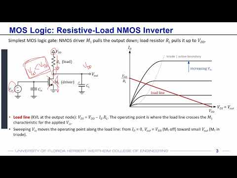
- With an NMOS source grounded and a drain load connected to VDD, Vin below threshold turns the transistor off.
- When the NMOS is off, there is no DC path through the load, so the drain output stays near VDD.
- A sufficiently high input turns on the NMOS and discharges the output node, producing an inverted logic level.
- The inverter maps a low input to a high output and a high input to a low output, giving a 180-degree inversion.
- Near threshold, the NMOS initially operates in saturation because VDS is large relative to its overdrive voltage.
- As Vin rises and Vout falls, the transistor enters triode, pulling the output toward ground.
- For an NMOS NOR gate, either input being high turns on a parallel transistor and discharges the output.
- For an NMOS NAND gate, both inputs must be high to complete the series path that discharges the output.
- When no NMOS discharge path is active, a resistor load charges the output capacitance toward VDD.
- When a resistor-loaded NMOS output is low, current flows continuously from VDD through RL to ground.
- The static current is approximately (VDD - VOL)/RL, so increasing RL reduces current but increases the output RC charging time.
- The tradeoff between static power and slow charging motivates replacing the resistor load with a PMOS transistor.
- With Vin at zero, the NMOS is off and the PMOS is on, charging the output capacitance toward VDD.
- With Vin at VDD, the NMOS is on and the PMOS is off, discharging the output toward ground.
- The complementary devices form a CMOS inverter without a continuous resistor-to-ground path in either steady logic state.
- In triode, the NMOS drain current follows ID = K[(VGS - VT)VDS - VDS²/2].
- Differentiating with respect to VDS gives GDS = K(VGS - VT - VDS), with small-signal on-resistance equal to 1/GDS.
- For a strongly on transistor with small VDS and VGS near VDD, Ron is approximately 1/[K(VDD - VT)].
- The NMOS pull-down network implements the output-discharge condition; the PMOS pull-up network implements its dual.
- For a CMOS NOR gate, parallel NMOS devices discharge for either high input, while series PMOS devices charge only when both inputs are low.
- For a CMOS NAND gate, series NMOS devices discharge only when both inputs are high, while parallel PMOS devices provide the pull-up path.
- Charging a capacitance C from 0 to VDD draws charge CVDD from the supply and draws energy CVDD².
- The capacitor stores half CVDD²; the other half is dissipated during charging, and the stored half is dissipated during discharge.
- A full charge-discharge cycle therefore dissipates CVDD², giving the approximate switching-power relation P = CVDD²f.
- Low-to-high and high-to-low propagation delays are measured to the halfway point, VDD/2.
- Rise time is measured from 0.1VDD to 0.9VDD, while fall time is measured from 0.9VDD to 0.1VDD to reduce sensitivity to noise.
- The lecture gives approximate RC estimates of 0.69RC for propagation delay and 2.2RC for rise or fall time, with derivations planned for the next lecture.
Transcript excerpt
0:01 All right. So, um as we get started with lab seven this week, uh we would like to spend some time on uh the contents of lab 7, which is basically how do you design digital circuits with uh transistors that you have learned so far. Uh we have looked into different type of analog circuits. But just for today's lecture, we'll look into how do you do digital design with the transistors that you have already learned and what are the considerations in digital design which basically are the contents of your lab 7. Um your homework eight will also be related to that as you have talked about in the previous lecture. Uh that your homework eight which would be due on November 30th which is two weeks from now is based on those digital design concepts. Um and then from the next lecture onwards we'll go back to our opam
0:49 design. We have been discussing about how do you design an OPM um in the last lecture and we'll go back to those discussions from Wednesday onwards. So we are going to have two lectures which will be dedicated towards design of the opamp and homework nine will be a um we'll deal with the actual design of the opamp as an example. Um so for today's lecture we'll go back to um we'll take a d2 a slide detour which talks about simos logic circuits or digital design using transistors. So the first question is if you're an analog circuit designer versus a digital circuit designer, what do you want? And we have talked about this a little bit over uh the previous lectures. But as an analog designers, you want to keep the
1:38 transistors in saturation. Why do you want the transistor in saturation? Because only in saturation you're going
This is the start of the transcript. Save this video free for the whole transcript, searchable and time-coded.
In this course
Related notes
Summary, takeaways, and chapters were generated by AI from the video's transcript and may contain errors. The video belongs to its creator, WISE Lab - UF ECE.