ECircuits-Lec15-2026
Overview
The lecture introduces semiconductor diodes as components behind non-ideal behavior in op amps, progressing from the ideal short/open-circuit model to how a silicon PN junction conducts. It explains silicon bonding and doping, majority and minority carriers, depletion-region changes under forward and reverse bias, and why real diodes show a forward turn-on curve and reverse leakage.
Key takeaways
- An ideal diode acts as a zero-resistance short in forward bias and an infinite-resistance open circuit in reverse bias, but real diodes depart from both extremes.
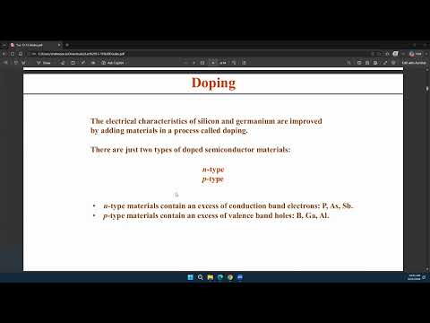
- Doping silicon with phosphorus, arsenic, or antimony creates N-type material with electrons as majority carriers; boron, gallium, or aluminum creates P-type material with holes as majority carriers.
- A PN junction’s depletion region forms when electrons and holes recombine near the interface, leaving immobile ions but few mobile carriers.
- Reverse bias pulls majority carriers away from the junction and widens the depletion region, while forward bias pushes carriers toward the junction and shrinks it.
- Real diodes have a nonlinear forward turn-on characteristic and a small reverse leakage current caused by minority carriers; the lecture gives nanoamperes or picoamperes as typical leakage scales.
Chapters
- Homework 3 is due tonight and Exam 1 is due next week.
- Lab 3 has a two-week completion window, also intended for catching up on earlier lab material.
- The lecture begins studying diodes as components that help explain non-ideal behavior inside op amps.
- Unlike a reciprocal resistor, a diode is unilateral: it permits current in one direction and blocks it in the other.
- The ideal forward-biased diode is modeled as a short circuit with zero voltage and zero forward resistance.
- The ideal reverse-biased diode is modeled as an open circuit with zero current and infinite reverse resistance.
- Silicon, germanium, and gallium arsenide are introduced as semiconductor materials with conductivity between metals and insulators.
- Gallium nitride is noted as a material used in high-power applications where silicon may not withstand the voltage or current.
- Semiconductor conductivity can be altered by material composition and the presence of mobile charge carriers.
- Silicon has 14 electrons, arranged in the lecture’s simplified shell model as 2, 8, and 4.
- Each silicon atom forms covalent bonds with four neighboring atoms, creating a stable crystal structure.
- Energy can free outer-shell electrons to move through the material; the number of mobile carriers affects conductivity.
- Doping adds impurities to silicon to change the number of mobile charge carriers.
- Phosphorus, arsenic, and antimony have five outer-shell electrons; an extra electron makes the doped material N-type.
- Boron, gallium, and aluminum have three outer-shell electrons; the missing electron acts as a mobile hole in P-type material.
- Electrons and holes both contribute to electrical conduction.
- A PN junction forms when P-type and N-type regions meet in the same semiconductor material.
- P-type material has holes as its majority carriers, while N-type material has electrons as its majority carriers.
- Doping changes the available mobile carriers, not the overall electrical neutrality of the material.
- Minority carriers also exist: electrons in P-type material and holes in N-type material.
- When P-type and N-type regions meet, holes and electrons diffuse toward the junction and recombine.
- Recombination leaves a depletion region near the interface with few mobile electrons or holes.
- Immobile charged ions remain in the depletion region, so depletion means a lack of mobile carriers, not a lack of charge.
- A depletion region exists even when no external bias is applied.
- Reverse bias applies a negative voltage to the P side and a positive voltage to the N side.
- The battery draws majority carriers away from the junction: holes leave the P region and electrons leave the N region.
- As those carriers move away, the depletion region widens and increasingly impedes current flow.
- Current is the rate of charge movement, so a region without mobile carriers cannot sustain significant current.
- Forward bias connects positive voltage to the P side and negative voltage to the N side, pushing holes and electrons toward the junction.
- As the depletion region shrinks, carriers can cross the junction and recombine, producing substantial current.
- A real diode does not conduct strongly at an arbitrarily small forward voltage; its current rises sharply after the depletion barrier is sufficiently reduced.
- The ideal diode’s immediate turn-on model therefore differs from the gradual, nonlinear forward characteristic of a real diode.
- Real diodes carry a small reverse leakage current because minority carriers can cross the junction under reverse bias.
- The lecture contrasts reverse leakage, often in the nanoampere or picoampere range, with forward current that can reach milliamperes or hundreds of milliamperes.
- The closing discussion addresses access to the lecture playlist and a mixed-signal course prerequisite, with digital design or E-Circuits 1 mentioned.
- A student asks how removing holes and electrons expands the depletion region; the remaining junction-bias question is taken up for further discussion.
Transcript excerpt
0:03 Okay, so just brief announcements. All of you know homework three, that's due tonight. Exam one, that's due next week. And lab three, because we have the homework three due this week and the exam due next week, what we're doing is that we're we're giving two weeks of time to complete lab three. So if you want if you are able to if you're already done with homework and the lab, homework and the exam, then you can probably just go ahead and do your lab three next week. But if you don't want to do it in the next week, you can do it in the week after as well. So both of those weeks will be used for and utilized for lab three. And this should be a good time to if you're trying to catch up with some of the lab material, if you have missed anything in the previous two labs, this would be a
0:51 good time to catch up as well. Any questions? So if not, from today's lecture we're going to start looking into different types of devices that can be present inside an op amp. By now you probably have a very good idea about how non-ideal op amps operate and what are the kind of non-idealities we can expect from the op amp. But we still don't know that why are these non-idealities there? Why do they exist? And that eventually will boil down to some of the components that will be there in an op amp IC. And those components could be let's say two terminal devices like diodes, it
1:40 could be three terminal or four terminal devices like BJTs or MOSFETs as well. And we're going to learn about those devices in the next few weeks. So today's lecture
This is the start of the transcript. Save this video free for the whole transcript, searchable and time-coded.
In this course
Related notes
Summary, takeaways, and chapters were generated by AI from the video's transcript and may contain errors. The video belongs to its creator, WISE Lab - UF ECE.