ECircuits-Lec33-2026
Overview
The lecture develops the MOS differential amplifier from differential signaling fundamentals to a practical NMOS differential pair with a tail current source. It explains common-mode noise rejection, derives branch and output behavior from the fixed tail current ISS, and establishes saturation and output-swing limits, including why differential output swing is twice the single-ended swing.
Key takeaways
- A differential signal requires opposite-phase AC excursions around a shared DC common-mode level; subtracting two nodes of amplitude VO produces a differential amplitude of 2VO.
- Differential outputs suppress common-mode disturbances such as clock-line crosstalk and supply noise, with cancellation limited by mismatch in coupling or circuit branches.
- A pseudo-differential pair lacks a tail current source, so input common-mode changes alter MOS overdrive, current, gm, output bias, and potentially saturation.
- For a matched differential pair with tail current ISS and equal DC inputs, each branch carries ISS/2 and the output common-mode level is VDD - RD·ISS/2.
- A differential pair steers nearly all ISS into one branch when its input DC difference is large enough to turn off the other transistor; the outputs then approach VDD and VDD - RD·ISS.
- The input common-mode range must leave enough voltage for both the input transistor’s VGS and the tail device’s saturation overdrive, while output swing is constrained by the input transistors’ saturation condition.
Chapters
- A single-ended signal is measured relative to ground, while a differential signal is the voltage difference between two nodes with equal-and-opposite AC excursions.
- The two inputs share a common-mode DC bias so their difference represents the AC signal rather than an unwanted DC offset.
- If each node has amplitude VO, its single-ended peak-to-peak swing is 2VO; subtracting opposite-phase nodes gives a differential amplitude of 2VO and peak-to-peak swing of 4VO.
- Parasitic capacitance between nearby metal lines can couple a rail-to-rail clock transition onto an amplifier output and distort its sine wave.
- With differential victim lines, similar clock noise couples onto both outputs and largely cancels when one output is subtracted from the other.
- Cancellation is strongest when the parasitic capacitances and coupling are matched; layout mismatch leaves residual noise.
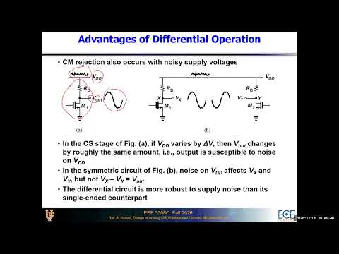
- Noise on VDD can appear at the output of a single common-source amplifier, even when its input is a clean sine wave.
- A differential pair rejects noise shared by VX and VY while retaining their opposite-phase signal components.
- In crosstalk terminology, the clock is the aggressor and the amplifier output is the victim; making victim signals differential is generally easier than converting every aggressor to differential signaling.
- For a common-source branch with load RD, the output’s maximum single-ended peak-to-peak swing is limited to approximately VDD minus the minimum transistor VDS.
- NMOS saturation requires VDS to be at least the overdrive voltage, VOV = VGS - VTH, giving a swing limit of VDD - VOV.
- Subtracting the two differential outputs doubles the effective swing to approximately 2(VDD - VOV).
- Two common-source stages driven by opposite-phase inputs form a basic differential-looking circuit, but each branch current still depends on its input’s DC gate voltage.
- The MOS current follows ID = (K/2)VOV², so changing the input common-mode level changes VOV, branch current, and transconductance gm = K·VOV.
- Excessive input bias can raise current enough to lower transistor VDS below VOV, while too little bias can turn a transistor off and push the output common-mode voltage toward VDD.
- Adding a tail current source ISS fixes the total current drawn by the two branches, unlike the pseudo-differential circuit.
- For matched transistors and equal DC inputs, each branch carries ISS/2 and each output common-mode voltage is VDD - RD·ISS/2.
- Because VOV is determined by current, approximately VOV = √(2ID/K), fixing the tail current makes branch bias less dependent on input common-mode voltage.
- The tail source can be implemented with a MOS current mirror, including a diode-connected reference transistor; the pair with this source is the practical differential pair.
- When the DC inputs are equal, the matched branches split ISS evenly and both outputs sit at VDD - RD·ISS/2.
- If one input becomes sufficiently lower than the other, its transistor turns off and the other branch carries nearly all of ISS.
- The inactive branch output rises to VDD, while the conducting branch output falls to VDD - RD·ISS.
- The balanced operating point is at VIN1 - VIN2 = 0; a DC differential input shifts the outputs away from their equal common-mode bias.
- The tail current source must remain in saturation, requiring its drain-to-source voltage to exceed its overdrive voltage.
- The input common-mode voltage must be high enough to provide both the input transistor’s required VGS and the tail transistor’s minimum saturation voltage, approximately VGS1 + VOV3.
- Once the devices are on and in saturation, increasing input common-mode voltage moves the shared source node VP upward rather than changing the fixed tail current.
- Below the required common-mode range, branch currents and output common-mode voltage are no longer constant because devices may be off or out of saturation.
- Each output can rise toward VDD, but the NMOS drain voltage must remain above VG - VTH to keep the input transistor in saturation.
- The lowest output level is therefore approximately VIN,CM - VTH; the input common-mode voltage itself cannot fall below the level needed to support the tail device and input transistor.
- The resulting single-ended peak-to-peak output swing is approximately VDD - (VGS1 - VTH1) - (VGS3 - VTH3), under the stated minimum-bias assumptions.
- The differential peak-to-peak swing is twice the single-ended swing because the two outputs move in opposite directions.
- The lecture concludes after deriving the differential pair’s operating regions, common-mode behavior, and output swing constraints.
- The planned follow-up covers large-signal DC analysis, small-signal AC analysis, and worked differential-pair examples.
Transcript excerpt
0:00 recording the meeting as well. So as I mentioned in the class, I'm traveling today. So you might hear a little bit of crosstalk in the background, but please bear with me. So I'll I'll try to make sure that yeah, we are covering all the important topics about differential amplifiers today. Now till now we have discussed about single-ended amplifiers. We have discussed common source, common gate, common drain topologies. Now what is the difference between single-ended and differential first of all? So if we think about it, let me see if I yes. So if we think about it, differential versus single-ended has a few differences between them. So first of
0:48 all, a single-ended signal is a signal that is measured with respect to a fixed reference potential. So usually that's the ground or the reference point. Now on the other hand, a different signal differential signal is measured between two defined nodes. Now important thing is that even for single-ended, you are measuring the signal between two nodes. One is your signal or the voltage node and the other one is the ground. However, the differential signal is a little bit different. A differential signal is between two nodes that have equal and opposite signal excursions. So that is the important thing to remember for differential signaling that a single-ended signal does not mean that it's also differential because it is taken between a signal node and a ground
1:36 because for differential signaling, you need to have two nodes. In one node, if you're having a sine wave, a positive going sine wave, on the other node, you need to have a negative going sine wave. So you should have a positive half cycle of the sine wave for the first node, while the second node has the negative
This is the start of the transcript. Save this video free for the whole transcript, searchable and time-coded.
In this course
Related notes
Summary, takeaways, and chapters were generated by AI from the video's transcript and may contain errors. The video belongs to its creator, WISE Lab - UF ECE.