EE 330 Lecture 2026 11 12 Ch7 Amp#4
Overview
The lecture develops small-signal analysis for BJT and MOSFET amplifiers, showing how DC bias establishes device parameters and how AC equivalents support gain calculations. It derives the behavior of six basic configurations, including common-emitter and common-source gains of approximately −gmRC and −gmRD, and explains why input and output resistance matter when connecting amplifier stages.
Key takeaways
- Small-signal analysis begins with the DC operating point: for the example with IE = 1 mA and β = 100, IC is about 0.99 mA and IB about 0.01 mA.
- The simplified voltage gains are approximately −gmRC for common-emitter, +gmRC for common-base, −gmRD for common-source, and +gmRD for common-gate.
- Common-drain MOSFET and common-collector BJT stages have gain gmRL/(1 + gmRL), which approaches unity when gmRL is large.
- A BJT hybrid-pi model uses rπ and a controlled current source, while the T model uses emitter resistance re; both represent the same small-signal behavior.
- Amplifier stages should generally present high input resistance to avoid loading their sources and low output resistance to deliver signal efficiently to a load.
- To calculate resistance with a test source, deactivate independent sources but retain dependent sources; use Rout = vx/ix at the output and Rin = vtest/itest at the input.
Chapters
- After informal classroom conversation, the lecture begins at about 1:46 and notes that the class is meeting in a smaller room.
- The topic is Chapter 7 amplifier analysis, especially small-signal models for BJT and MOSFET circuits.
- For AC analysis, DC voltage sources become shorts and coupling capacitors are treated as short circuits.
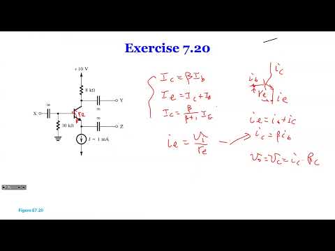
- The BJT current relations remain useful for small signals: ic = βib and ie = ic + ib, with α relating collector and emitter current.
- To find gain, relate the emitter current to the small-signal voltage across re, then calculate the collector output using the collector resistance RC.
- A transistor can be classified by which terminal is common to the input and output; changing the chosen terminals changes the amplifier configuration.
- The example labels three terminals X, Y, and Z, with the input at X and output selectable at Y or Z.
- A collector load or emitter current source can make a circuit less like the simplest textbook common-emitter, common-base, or common-collector arrangement.
- For DC, capacitors are open circuits, so the example is first reduced to its bias circuit.
- With emitter current IE = 1 mA and β = 100, the lecture estimates IC at about 0.99 mA and IB at about 0.01 mA.
- The DC collector current supplies the operating point needed to calculate small-signal parameters such as gm and rπ.
- For AC analysis, ideal DC current sources are opened, but doing so naively can leave the example without a valid path for signal current.
- The model retains the transistor Early-effect resistance ro, which provides an AC path in the equivalent circuit.
- The lecture distinguishes the DC bias source from the transistor's small-signal controlled current source and output resistance.
- The small-signal model replaces the BJT with rπ between base and emitter and a controlled collector current source.
- The example places a 10 kΩ resistance on the input side, an 8 kΩ collector resistance, and ro at the emitter-side connection.
- Because rπ and the emitter-side resistance are not simply in series or parallel in this circuit, the lecture relates terminal voltages and currents algebraically.
- The voltage across rπ is vb − ve = ib rπ, while the emitter voltage is ve = ie ro in the illustrated model.
- Using ie = (β + 1)ib yields an equivalent emitter-side resistance of approximately (β + 1)ro when referred through the current relation.
- After finding ve and ib, calculate ic = βib and the collector output from the drop across RC; these steps produce the voltage gain.
- The MOSFET small-signal model uses a controlled current gm vgs and output resistance ro.
- The BJT hybrid-pi and T models express the same device behavior in different forms, with parameters such as rπ, re, gm, and β.
- The instructor recommends keeping model equations available and practicing their use rather than relying only on memorization.
- For AC analysis, DC supply rails become ground, even though the MOSFET still needs an appropriate DC drain bias.
- Common-source uses the source as the common, AC-grounded terminal; common-gate grounds the gate and typically takes input at the source.
- Common-drain takes output at the source, while the drain is AC-grounded through the DC supply.
- For a common-source stage with input at the gate and output at the drain, vo = −gmvgsRD, giving Av ≈ −gmRD.
- For a common-gate stage, the input is at the source and vgs = −vi, so the gain is approximately +gmRD.
- The common-source output is inverted, while the common-gate output is in phase with its input in the simplified model.
- In a common-drain stage, the drain is AC-grounded and the output is taken across the source load RL.
- Because vgs = vi − vo, solving the feedback relation gives Av = gmRL / (1 + gmRL).
- When gmRL is large, the gain approaches 1, so the stage is called a source follower and is useful for changing input and output resistance.
- The simplified common-emitter gain is approximately −gmRC, while the common-base gain is approximately +gmRC.
- For the common-collector stage, the emitter output is not identical to the base input; using ve = vi − vo gives Av ≈ gmRL / (1 + gmRL).
- When gmRL is large, the common-collector gain approaches unity and the stage is called an emitter follower.
- A sensor's internal resistance can reduce the signal reaching an amplifier input, especially when the amplifier input resistance is not sufficiently high.
- A large input resistance minimizes loading, while a small output resistance helps deliver more of the amplifier's output to the next load.
- MOSFET inputs ideally draw no gate current, and source followers can help provide a low-resistance output for later stages.
- To find output resistance, short independent voltage sources, open independent current sources, preserve dependent sources, apply a test voltage, and calculate Rout = vx/ix.
- To find input resistance, apply a test voltage at the input and divide it by the resulting input current; leave the output open.
- In the illustrated BJT common-emitter example, Rout is RC and Rin is rπ; the ideal MOSFET gate input resistance is infinite because its input current is zero.
- The lecture closes by emphasizing derivation procedures over memorizing the six gains and twelve input/output resistance formulas.
Transcript excerpt
0:05 My teacher does not like, okay, >> assum It's true. >> No, I I see it. I see it. Like it is true. And like we just don't know like initially like so I just Okay.
0:54 and he's like so long time >> you could have just two sentence answer because it's somewhere where like I It's It's very like I think
1:46 >> we'll get started. Like we have a smaller classroom today. The grid's getting bigger. It's crazy. Go somehow. Yeah. So um sometimes when we solve uh
2:52 small signal problem um the best approach is right in the beginning is to draw the small signal current circuit and then analyze the circuit to get your numerical solution. But once you get familiar with this system like how to do it sometimes you don't even have to draw the small signal circuit. you can directly show for the parameters that you want on the uh BJT or MOSFET device circuit cell. Now for example this this is the example that we had um on Tuesday right? So we had a GMT BJT and it works. It works through as amplifiers have
3:41 input at the base ground which is common amplifier then we have all output at the I me to draw normally but make sure that your which didn't make any. So the connector is on the right hand and on the bottom. So that's how you draw the circuit. Now if you look at the circuit for AC the DC voltages become a short circuit. So it become the ground or voltage source become circuit one side is connected. So you come down. So uh
4:31 and then of course you have your bases around it and your input uh initially we have a capacitor here but AC capacitor
This is the start of the transcript. Save this video free for the whole transcript, searchable and time-coded.
In this course
Related notes
Summary, takeaways, and chapters were generated by AI from the video's transcript and may contain errors. The video belongs to its creator, Wireless Power Transfer.