ECircuits-Lec22-2026
 Watch on YouTube →
Overview
The lecture introduces MOSFET structure and operation, comparing the devices with BJTs and explaining how a gate voltage creates a conductive channel between source and drain. It covers N-channel and P-channel doping, gate-oxide coupling, transistor symbols, CMOS use, width-to-length ratio, and the basic output I-V regions, with detailed current equations deferred to the next lecture.
Key takeaways
- A MOSFET controls source-to-drain current primarily through gate voltage, unlike the BJT current-control model introduced for comparison.
- An N-channel MOSFET uses N-type source and drain regions in a P-type body and forms an electron channel when its gate voltage exceeds the threshold.
- Conventional current direction depends on the majority carrier: it flows drain to source in an N-channel MOSFET and source to drain in a P-channel MOSFET.
- The gate oxide isolates the gate from the semiconductor while enabling capacitive coupling, so the gate can modulate channel charge without directly shorting to the body.
- MOSFET designers choose W/L, the width-to-length aspect ratio, as a key transistor sizing parameter.
- In CMOS logic, P-channel devices commonly form the pull-up network and N-channel devices the pull-down network, charging or discharging the output capacitance.
Chapters
0:00
Lab Four Schedule and the Shift from BJTs to MOSFETs
- Lab Four is similar to Lab Three and has a two-week completion window because it requires MOSFET knowledge.
- Labs Five, Six, and Seven remain after Lab Four, with the goal of finishing labs before Thanksgiving break.
- The course begins MOSFETs before returning to BJT small-signal and AC analysis; a recorded 2024 lecture set covers the omitted BJT material.
2:15
MOSFET Terminals and Voltage-Controlled Operation
- MOSFETs have source and drain terminals for the main current path, a gate that controls current, and a body or bulk terminal.
- The body is the silicon substrate supporting the device; its bias can affect operation even though source, drain, and gate are the key functional terminals.
- Unlike a BJT, which is introduced as a current-controlled device, a MOSFET is controlled by voltage at its gate.
5:12
Source, Drain, and Conventional Current Direction
- Source and drain are named for the movement of majority carriers: those carriers move from source toward drain.
- In an N-channel MOSFET, electrons move source to drain, so conventional current flows drain to source.
- In a P-channel MOSFET, holes move source to drain, so conventional current flows in the same direction.
- BJT and MOSFET circuit analysis share many methods, though their physical structures and some governing equations differ.
10:30
MOSFET Layout, Contacts, and Active Regions
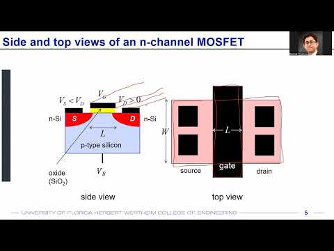
- The top view shows an active region with source and drain on opposite sides of a gate; the side view reveals the device cross-section.
- Multiple metal contacts connect the source and drain regions to external circuitry.
- Multiple contacts reduce effective contact resistance by placing contact resistances in parallel and improve the chance that at least some nanoscale contacts work.
15:20
N-Channel Substrate Doping and Device Fabrication
- An N-channel MOSFET has N-type source and drain regions formed in a P-type body; a P-channel MOSFET reverses those doping types.
- A typical fabrication explanation starts with a P-type silicon wafer and selectively adds phosphorus through masked ion implantation to form N-type regions.
- The lecture distinguishes circuit-level device behavior from fabrication details such as masking, ion implantation, and diffusion.
21:57
Gate Oxide, Capacitive Coupling, and W/L Geometry
- Silicon dioxide electrically isolates the metal gate from the semiconductor, preventing a direct short while allowing capacitive coupling.
- A gate voltage couples through the oxide to influence charge beneath the gate and thereby control source-to-drain conduction.
- W is the transistor width and L is the gate length; their ratio, W/L, is the MOSFET aspect ratio selected by circuit designers.
27:00
Threshold Voltage Creates N-Channel and P-Channel Paths
- For an N-channel device, a positive gate voltage above the threshold voltage attracts electrons beneath the gate and forms a channel connecting source and drain.
- For a P-channel device, a sufficiently negative gate voltage attracts holes and creates a P-type channel in the N-type body.
- The channel is induced during operation rather than present initially in the enhancement-mode devices emphasized in the lecture.
- Conventional current enters the drain of an N-channel MOSFET and leaves the drain of a P-channel MOSFET.
33:35
MOSFET Symbols, Enhancement Mode, and CMOS Logic
- A dashed channel in a MOSFET symbol indicates enhancement mode, where the channel forms only after the gate reaches the required voltage; modern symbols often use a solid line.
- The source arrow indicates conventional current direction, while some digital-circuit diagrams mark P-channel devices with a gate bubble.
- CMOS combines P-channel and N-channel MOSFETs, commonly placing the P-channel pull-up network above the N-channel pull-down network.
- In digital logic, the pull-up network charges an output capacitance toward VDD and the pull-down network discharges it toward ground.
43:22
MOSFET Output I-V Curves and Operating Regions
- For a common-source circuit with the source grounded, VGS means VG minus VS and VDS means VD minus VS; the output characteristic plots drain current against drain-to-source voltage.
- At a fixed VGS, drain current first rises in the linear or triode region and then becomes approximately constant in saturation.
- Increasing VGS raises the saturation current, making the saturated MOSFET behave approximately as a gate-controlled current source; cutoff corresponds to current near zero.
- The lecture ends before deriving the I-V equations, previewing energy-band analysis and mathematical derivation for the next class.
Summary, takeaways, and chapters were generated by AI from the video's transcript and may contain errors. The video belongs to its creator, WISE Lab - UF ECE.