ECircuits-Lec21-2026 (self-study: BJT part 2)
 Watch on YouTube →
Overview
The lecture maps BJT circuit analysis onto familiar MOSFET techniques, deriving key small-signal quantities and showing how to analyze common-emitter and emitter-follower stages. It gives practical formulas—such as g_m = I_C/V_T, r_π = β/g_m, and r_e ≈ 1/g_m—then works through a bias-and-gain example and explains why BJTs remain useful in high-frequency circuits.
Key takeaways
- At room temperature, BJT transconductance is g_m = I_C/25 mV, so a collector current of 2.3 mA yields about 92 mS.
- The BJT small-signal base resistance is r_π = β/g_m, while the emitter resistance is approximately 1/g_m; these replace the MOSFET's nearly infinite DC gate resistance in input analysis.
- Emitter degeneration increases the base input resistance to r_π + (1+β)R_E and reduces effective transconductance to approximately g_m/(1+g_mR_E).
- For β = 100, α = β/(1+β) ≈ 0.99, explaining why collector current is nearly equal to emitter current.
- A 3 V base supply through 100 kΩ, with V_BE = 0.7 V and β = 100, produces I_B = 23 μA and I_C = 2.3 mA; with a 3 kΩ collector resistor and 10 V supply, V_CE is 3.1 V.
- BJT and MOSFET amplifier configurations share analysis patterns, but BJTs are especially relevant to high-frequency design because their device structure and gain characteristics can suit millimeter-wave applications.
Chapters
0:00
Course Wrap-Up, Divide-and-Conquer Analysis, and Final Exam Guidance
- Electronic-circuit analysis relies on breaking large systems into smaller diode, MOSFET, and BJT stages.
- The final exam is scheduled for December 10 at 10:00 a.m.; homework sets 4–9 are highlighted as important preparation.
- The lecture frames circuit fundamentals as building blocks for more complex industry designs.
3:15
Mapping BJT Terminals and Symbols to MOSFETs
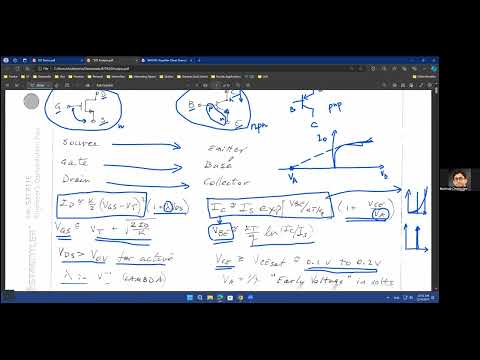
- The base corresponds functionally to the MOSFET gate, the emitter to the source, and the collector to the drain.
- BJT symbols place an arrow on the emitter; its direction indicates conventional emitter-current direction.
- The lecture compares NPN with n-channel MOSFETs and PNP with p-channel devices.
5:30
BJT Exponential Current, Early Voltage, and Active-Region Conditions
- The collector current follows an exponential dependence on base-emitter voltage: I_C ≈ I_S e^(V_BE/V_T), with an Early-effect correction.
- The BJT Early voltage V_A is the extrapolated output-characteristic intercept, with λ = 1/V_A.
- Because V_BE changes by only roughly 100–200 mV across large current ranges, circuit analysis often approximates the forward-biased junction drop as about 0.7 V.
- For the lecture's practical active-region check, V_CE should remain above roughly 0.1–0.2 V.
10:00
BJT Transconductance, Output Resistance, and Intrinsic Gain
- Small-signal transconductance is g_m = ∂I_C/∂V_BE = I_C/V_T; at room temperature V_T is about 25 mV.
- The Early-effect output resistance is r_o = V_A/I_C, analogous to MOSFET r_o = 1/(λI_D).
- BJT intrinsic gain is g_m r_o = V_A/V_T, connecting the Early voltage directly to voltage-gain capability.
14:08
Base Current, β, and Common-Emitter/Common-Base Gain
- Unlike the insulated MOSFET gate, a BJT base draws current; the approximation is I_B = I_C/β.
- Common-emitter current gain is β = I_C/I_B, while common-base gain is α = I_C/I_E.
- The gains are related by α = β/(1+β) and β = α/(1−α); for β = 100, α is about 0.99.
- Common-emitter and common-base configurations parallel the MOSFET common-source and common-gate arrangements.
19:54
Deriving BJT Small-Signal Input and Emitter Resistances
- The base-emitter small-signal resistance is r_π = β/g_m, representing the finite input resistance absent at an ideal MOSFET gate.
- The resistance looking into the emitter is r_e = α/g_m, commonly approximated as 1/g_m because α is close to 1.
- The derivation applies a test voltage at the emitter and relates its current to the base-emitter small-signal model.
28:33
Common-Emitter Emitter Degeneration and Effective Transconductance
- With a physical emitter resistor R_E, the base input resistance is r_in = r_π + (1+β)R_E.
- Since r_π ≈ βr_e, the emitter resistance appears amplified by approximately β when viewed from the base.
- Emitter degeneration reduces effective transconductance to approximately g_m/(1+g_mR_E), analogous to MOSFET source degeneration.
36:04
Emitter-Follower Gain and Output Resistance
- The emitter follower is the BJT counterpart of the MOSFET source follower, with the collector at AC ground and output at the emitter.
- Its voltage gain is approximately g_mR_eq/(1+g_mR_eq), typically near unity.
- Looking into the emitter gives approximately 1/g_m; a more complete estimate includes base resistance as 1/g_m + R_B/β.
41:02
Worked BJT Bias Point and Small-Signal Gain Example
- With a 3 V base supply, 100 kΩ base resistor, β = 100, and V_BE = 0.7 V, the example finds I_B = 23 μA and I_C = 2.3 mA.
- A 3 kΩ collector resistor drops 6.9 V from a 10 V supply, leaving V_CE = 3.1 V and keeping the transistor in forward-active operation.
- The operating current gives g_m ≈ 92 mS and r_π ≈ 1.09 kΩ; voltage gain includes input division across 100 kΩ and r_π, followed by the collector-stage gain.
47:00
BJT Applications, High-Frequency Advantages, and Course Close
- The lecture says BJT questions are excluded from the final exam but recommends BJT preparation for analog-design interviews at Texas Instruments and Analog Devices.
- BJTs lack the MOSFET gate-insulator capacitor but still have parasitic capacitances, so high-frequency behavior remains a design consideration.
- The lecture identifies high gain and high-frequency performance as reasons BJTs are used in millimeter-wave, 5G, and 6G circuit applications.
Summary, takeaways, and chapters were generated by AI from the video's transcript and may contain errors. The video belongs to its creator, WISE Lab - UF ECE.