ECircuits-Lec23-2026
 Watch on YouTube →
Overview
The lecture develops an intuitive and mathematical account of n-channel MOSFET operation, connecting energy-band diagrams and gate-controlled channel formation to the linear and saturation regions of the drain-current characteristic. It derives the oxide capacitance per unit area, channel charge, and a simplified current equation, then gives the gradual-channel result; course updates move the midterm to October 26 to 30 and keep Lab 4 open for two weeks.
Key takeaways
- In an nMOS, a positive gate voltage attracts electrons to the p-type channel and lowers the source-to-drain energy barrier; conduction begins when VGS exceeds VT.
- The overdrive voltage VOV = VGS - VT is the portion of the gate voltage available to form channel charge after threshold has been reached.
- The oxide capacitance per unit area is Cox = εox/tox, so thinner gate oxide increases gate coupling and the charge induced for a given voltage.
- The simplified linear-region model is ID ≈ μCox(W/L)(VGS - VT)VDS, showing that current scales with mobility, oxide capacitance, device width-to-length ratio, overdrive, and drain voltage.
- The gradual-channel equation includes a -VDS²/2 term, explaining why the linear current approximation must be corrected as drain voltage rises toward saturation.
- Lab 4 spans two weeks, and the midterm is scheduled for October 26 to 30 after MOSFET DC and AC analysis; Homework 4, Homework 5, and worked examples are planned beforehand.
Chapters
0:00
Lab 4 Flexibility and the Midterm Shift to October 26 to 30
- Lab 4 runs for two weeks, so students may attend in either week or split the work between both.
- The midterm moves from the week of October 19 to 23 to October 26 to 30 so MOSFET DC and AC analysis can be covered first.
- Homework 4, Homework 5, and example questions with answers are planned before the exam.
2:00
nMOS and pMOS Current Directions and Output Regions
- nMOS devices use electrons as majority carriers, while pMOS devices use holes.
- Electron motion in nMOS runs from source to drain, so conventional drain current flows from drain to source; pMOS conventional current flows from source to drain.
- The output characteristic plots drain current ID against drain-to-source voltage VDS, with cutoff, linear or triode, and saturation regions.
5:00
Gate Voltage Bends MOS Energy Bands and Creates an Electric Field
- A MOS stack contains a metal gate, a silicon dioxide insulator, and a semiconductor body.
- A positive gate voltage lowers electron energy by qV, bending both conduction and valence bands downward near the gate.
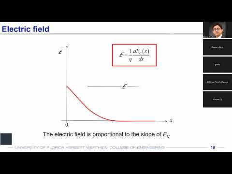
- Since E = -dV/dx and the energy slope is proportional to electric field, band bending also reveals the field profile through the MOS structure.
10:00
Positive Gate Bias Depletes Holes in the p-Type MOS Body
- A positive gate attracts electrons toward the oxide interface and repels holes from the p-type semiconductor.
- Carrier concentrations vary exponentially with band energy; the lecture contrasts this behavior on logarithmic and linear concentration axes.
- The interface region is called depletion because the majority-hole concentration falls sharply, even while minority-electron concentration rises.
15:00
Using Energy Bands to Read a p-n Junction
- In the n-type region, electron concentration is approximately the donor concentration ND; in the p-type region, hole concentration is approximately the acceptor concentration NA.
- The minority-carrier relations are presented as ni²/ND on the n side and ni²/NA on the p side.
- Band energy is lower on the electron-rich n side and higher on the p side; the band slope indicates electric field, while the middle depletion region has few mobile carriers.
20:00
Energy-Band Rules Prepare the nMOS Channel Model
- The lecture summarizes three diagram-reading rules: voltage is opposite in sign to electron energy, electric field follows the energy-band slope, and carrier density depends exponentially on band energy.
- An nMOS structure has n-type source and drain regions surrounding a p-type body and channel.
- The conduction and valence bands shift together across n-p-n regions while their energy separation remains constant.
28:00
Gate Bias Lowers the nMOS Source-to-Drain Barrier
- A positive gate voltage attracts electrons into the channel and lowers its energy barrier between the n-type source and drain.
- The gate-to-source voltage must exceed threshold voltage VT to form a conducting channel; the excess is the overdrive voltage VOV = VGS - VT.
- The lecture relates technology-node labels to shrinking source-to-drain dimensions, while noting that labels below 22 nm do not necessarily equal the physical gate length.
36:00
Drain Bias Drives Channel Electrons and Shapes the I-V Curve
- With the channel on, a positive drain voltage attracts source electrons toward the drain and creates a downhill energy profile along the channel.
- As VDS rises, drain current initially increases approximately linearly, then approaches the saturation region.
- The output curves depend on gate bias: larger gate voltage creates a stronger channel and a larger current for a given VDS.
42:00
Oxide Capacitance and Gate-Controlled Channel Charge
- The gate, silicon dioxide, and semiconductor form a capacitor, with oxide capacitance per unit area Cox = εox/tox.
- Reducing oxide thickness tox increases Cox, and the lecture gives farads per square centimeter as the unit.
- For VGS above VT, channel charge is controlled by the overdrive voltage VGS - VT; because channel potential changes from source to drain, charge varies with position x.
47:00
Deriving Simplified and Gradual-Channel nMOS Current Equations
- Current is charge density multiplied by carrier velocity and device width W; the channel length is L.
- Using carrier mobility μ and the average-field approximation VDS/L gives the linear-region model ID ≈ μCox(W/L)(VGS - VT)VDS.
- The gradual-channel result adds the drain-voltage correction: ID = μCox(W/L)[(VGS - VT)VDS - VDS²/2], which the next lecture will continue from.
Summary, takeaways, and chapters were generated by AI from the video's transcript and may contain errors. The video belongs to its creator, WISE Lab - UF ECE.