Section 5 FLASH Part 4
 Watch on YouTube →
Overview
Shimeng Yu explains why 2D NAND scaling stalled near 15 nm: shrinking floating-gate cells increased cell-to-cell interference, worsened few-electron retention, and tightened the voltage margins for multi-level storage. He traces the shift to 3D NAND using charge-trap MONOS cells, explains vertical-channel architecture and manufacturing, and follows industry scaling from Samsung’s 24-layer 2014 product to more than 300 layers today, with wafer bonding and stacking proposed for future designs beyond 1,000 layers.
Key takeaways
- 2D NAND’s scaling limit was not just lithography: at about 15 nm, stronger cell-to-cell capacitance and storage of only dozens of electrons made both programming interference and retention increasingly difficult.
- Reducing floating-gate overlap or inserting air gaps lowers coupling, but weaker control-gate coupling can demand higher programming voltage.
- Charge-trap MONOS cells use insulating silicon nitride to localize electrons, reducing the risk that a single leakage path drains all the charge as it can in a conductive polysilicon floating gate.
- Mainstream 3D NAND uses vertical channel pillars with horizontal surrounding word lines, and selects strings with individual string-select transistors while sharing word lines across a plane.
- Samsung commercialized 3D NAND with 24 layers in 2014; leading products now exceed 300 layers, while multi-deck etching and wafer bonding address the process challenges of further scaling.
- CBA wafer bonding shortens connections between the memory array and peripheral circuits, and multi-tier bonding is one proposed path toward more than 1,000 NAND layers.
Chapters
- Late-generation 2D NAND reached critical dimensions around 15 nm, where further lithographic scaling became difficult.
- 3D NAND relaxed the cell’s XY dimensions and increased density by stacking memory layers vertically.
- Earlier 2D generations also adopted double patterning, air gaps, MLC, and TLC to extend scaling and improve density.
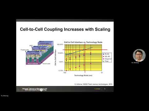
- Floating gates couple capacitively to neighboring cells, so changes in word-line or bit-line voltage can disturb stored charge.
- As floating-gate area shrinks, a cell may hold only dozens of electrons; losing one or two can shift its threshold voltage substantially.
- Stronger coupling and reduced charge populations make retention and reliability harder as 2D NAND approaches sub-20-nm dimensions.
- Page-by-page programming can shift an already programmed cell when an adjacent word line receives a high programming voltage.
- The resulting threshold-voltage shift can move distribution tails into neighboring MLC or TLC states, where voltage margins are narrow.
- The effect grows as adjacent cells move closer and their parasitic capacitance increases.
- Reducing floating-gate height or overlap area lowers intercell capacitance, but also weakens control-gate coupling and may require higher programming voltage.
- A planar control-gate geometry and lower-k silicon dioxide can reduce coupling between neighboring floating gates.
- Air gaps, with a dielectric constant near 1, reduce coupling more than silicon dioxide or silicon nitride and were used in late-generation 2D NAND.
- Random telegraph noise arises when electrons are trapped and detrapped near the gate-stack/channel interface, temporarily shifting threshold voltage.
- A dominant trap can cause roughly 100 to 200 mV of threshold-voltage change, a serious issue for TLC and QLC’s tight state margins.
- Lithography limits, cell interference, few-electron retention, and RTN helped motivate the industry’s move to 3D NAND and charge-trap cells.
- A floating gate stores charge in conductive polysilicon, while SONOS stores electrons in traps in an insulating silicon nitride layer between oxide layers.
- Because trapped electrons cannot readily move through the nitride, a localized leakage path is less likely to drain all stored charge than in a conductive floating gate.
- SONOS can offer lower programming voltage and improved endurance or retention, while retaining broadly similar program and erase schemes.
- Charge-trap structures evolved through names including MONOS, SONOS, and TANOS, reflecting changes in the gate and dielectric materials.
- Modern 3D NAND commonly uses a MONOS-style stack with a metal control gate, oxide/nitride/oxide charge-trap layers, and a silicon channel.
- During charge-trap erase, holes can enter the nitride and recombine with stored electrons; industry has also begun shifting some gate materials from tungsten toward molybdenum.
- The industry transition to 3D NAND began commercially around 2014 to 2015, after 2D NAND faced scaling and patterning limits.
- Simply repeating a complete 2D fabrication sequence for every layer saves substrate area but repeats costly lithography and processing.
- Toshiba’s 2007 bit-cost-scalable concept made vertical stacking practical by distributing fabrication cost across many memory cells.
- The architecture used in mainstream 3D NAND places a vertical channel inside horizontal, surrounding word-line gates.
- An alternative with horizontal channels and common vertical gates resembles stacked nanosheet logic, but is not the current mainstream NAND structure.
- Gate-first processing can support floating-gate designs, while gate-last processing is associated with charge-trap NAND; Solidigm’s lineage retains a floating-gate approach.
- Toshiba’s 2007 VLSI Symposium paper showed vertical channel pillars surrounded by stacked word lines, plus a staircase for word-line contacts.
- Each vertical string includes memory cells and string-select transistors at its ends, with the upper string-select line selecting an individual string.
- Word lines are shared across strings in a plane, so selecting a cell requires word-line control plus selection of the appropriate string and vertical slice.
- Each stacked word line needs an exposed landing pad so it can be contacted independently without shorting adjacent layers together.
- A single lithography mask defines the staircase’s first step; repeated photoresist trimming and etching expose successive word-line levels.
- As layer counts grow, the staircase consumes increasing peripheral area.
- Samsung’s 2009 VLSI Symposium design followed Toshiba’s vertical-channel concept and adopted a metal gate with a MONOS-style charge-trap stack.
- A memory pillar has an oxide-filled core, a polysilicon channel, an oxide/nitride/oxide charge-trap shell, and an outer metal gate.
- The pillars use a dense hexagonal layout, and the process forms stacked layers, etches vertical holes, deposits the channel and charge-trap layers, then replaces sacrificial nitride with metal gates.
- Conductive floating gates must be separated between cells to prevent stored electrons from migrating, while insulating nitride charge-trap layers can be continuous.
- Trap-cut structures have been proposed to isolate charge-trap cells as spacing and interference become concerns.
- Early 3D NAND used body erase through the silicon substrate; designs with isolated or metal-bonded arrays can use gate-induced drain leakage for erase.
- Samsung’s 2014 commercial generation used 24 layers and delivered a 128 GB chip configuration, making it the first company to bring 3D NAND to market.
- Cross-sections show the vertical core-shell pillars and staircase; the cell stack includes polysilicon, tunnel oxide, silicon nitride, and additional dielectric layers.
- A cylindrical 3D cell’s effective channel area scales with its perimeter and height, 2πR × H, making it larger than a roughly 15 nm by 15 nm planar cell and reducing interference.
- Samsung progressed from 24 layers in 2014 to 32 layers in 2015 and 64 layers in a later generation; current leading products exceed 300 layers.
- High-aspect-ratio holes are difficult to etch uniformly, prompting multi-deck approaches; one 96-layer design, for example, used two 48-layer decks.
- YMTC pioneered array/peripheral-circuit Xtacking, while wafer-to-wafer CBA bonding shortens interconnects compared with CUA routing.
- The cited areal-density progression rises from about 1 to roughly 30 Gb/mm², and multi-tier bonding is a proposed route toward designs exceeding 1,000 layers.
Transcript excerpt
0:05 So today we will continue the discussion on the flash memory and we will talk about the scaling challenges for the land flash. So here if you look at the scanning in terms of the real critical dimensions actually the land that's in the previous 2D era actually require more aggressive disography in terms of the smallest facial size. So the last few generations of the 2D land approaches the around 15 nanometer in the critical dimensions.
0:53 So today of course we know Dan is approaching like 12 nanometer but this was almost 10 years ago. So land already reach to about 15 nanometer and after that it's really difficult to scale. That's why industry switched to the 3D land which we will talk about today. But at that point the feature size actually got relaxed because the 3D land we will talk about that later to improve the density. We rely on more layers to be vertically stacked instead of pushing the scaling of the XY plane. So that's why the feature size actually got relaxed in the 3D n flesh.
1:44 So here if you look at the historical trend there are multiple innovations over the past 30 years in terms of the transistor fling gate transistor structure. So here as we discussed the transition happened almost 10 years ago 11 years ago and that's the last generation of the 2D land is about 1 Z node which is about 15 nanometer or so and uh yeah we discussed that for example the air gap has been introduced. Double patterning has been introduced to push the
2:33 critical dimension scaling and also the MLC TLC has been introduced to further improve the density. So if we review the scanning challenges in the previous 2D era. So we can summarize that into the following
This is the start of the transcript. Save this video free for the whole transcript, searchable and time-coded.
Related notes
Summary, takeaways, and chapters were generated by AI from the video's transcript and may contain errors. The video belongs to its creator, Shimeng Yu.