Lecture 4 DRAM Part 3
 Watch on YouTube →
Overview
Shimeng Yu explains how DRAM scaling depends on co-optimizing the 1T1C cell's storage capacitor, access transistor, and bitline capacitance. He traces current constraints, including roughly 5 fF storage capacitance, 0.4 to 0.5 nm equivalent oxide thickness, and capacitor aspect ratios above 80, then compares wafer-bonded 4F² vertical-channel cells with 3D DRAM stacking as routes beyond conventional 6F² scaling.
Key takeaways
- DRAM storage capacitance has declined only about eightfold, from roughly 40 fF in the late 1980s to 5 fF today, because bitline capacitance and sensing margin limit how far the cell can shrink.
- A high-k dielectric with k near 40 allows a physically 5 nm zirconium oxide layer to provide the capacitance of about 0.5 nm SiO2, while avoiding the leakage risks of an equally thin physical insulator.
- Capacitor aspect ratios above 80 create mechanical instability, so DRAM scaling depends on structural supports as well as dielectric and electrode innovations.
- Buried wordlines reduce bitline coupling by moving the wordline below the silicon surface, while air gaps reduce coupling by replacing higher-k material with a dielectric near 1.
- Wafer bonding enables separate optimization of the DRAM array and peripheral circuitry and supports 4F² vertical-channel concepts that hide the bit contact beneath the cell.
- 3D DRAM could extend density scaling through vertical stacking, but competitive density may require at least 64 layers and individually controlled wordlines, making fabrication substantially harder than stacked logic nanosheets.
Chapters
0:00
High-k Dielectrics Preserve DRAM Storage Capacitance
- DRAM capacitors evolved from silicon and silicon dioxide electrodes toward metal electrodes and high-k dielectrics, including zirconium oxide-based materials.
- Raising dielectric constant from about 4 for SiO2 to about 40 for zirconium oxide increases capacitance within a limited cell footprint.
- Storage capacitance fell from roughly 40 fF in the late 1980s to about 5 fF today, only an eightfold reduction despite much more aggressive dimensional scaling.
- Bitline capacitance changes relatively little across generations, so storage capacitance must remain high enough to preserve the cell's sensing margin.
8:00
EOT and the Capacitance-versus-Leakage Tradeoff
- Equivalent oxide thickness, or EOT, compares a high-k dielectric's capacitance with an SiO2 layer of equivalent electrical thickness.
- A 5 nm zirconium oxide layer with a dielectric constant near 40 has approximately the capacitance of 0.5 nm SiO2 with a dielectric constant near 4.
- Modern DRAM capacitors approach an EOT of 0.4 to 0.5 nm while retaining a physically thicker dielectric to avoid excessive leakage and tunneling.
- Very high-k materials can have smaller band gaps and lower electrode barriers, increasing leakage; the stated compromise is typically k of 30 to 40 and a band gap of 5 to 6 eV.
11:27
Pillar Capacitors Fit More Surface Area into Each Cell
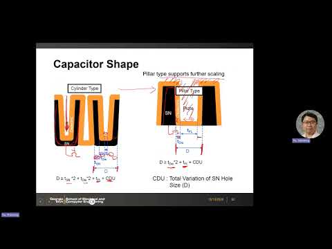
- The older cylinder capacitor uses a U-shaped storage-node electrode, dielectric, and opposing plate, consuming space for both electrode and dielectric thicknesses.
- The newer pillar-style geometry simplifies the critical dimension by reducing the electrode structure around the storage node.
- Capacitance depends on electrode surface area, so shrinking the cell perimeter requires taller capacitors to preserve area.
- Capacitor aspect ratios exceed 80 and can approach 100, creating mechanical-collapse risks that require structural support features.
18:12
Bitline Capacitance Comes from Several Coupling Paths
- Bitline capacitance includes coupling from the bit contact to the wordline, the bitline to the tall storage-node capacitor, and the bit contact to the substrate.
- Bit-contact-to-wordline and bitline-to-storage-node coupling are the largest components identified in the cell layout.
- Reducing bitline capacitance complements increasing storage capacitance because the sensing margin depends on the ratio of storage-node capacitance to bitline capacitance.
- A simple wire-to-wire coupling between neighboring bitlines is described as a smaller concern than the main contact and capacitor couplings.
23:56
Air-Gap Spacers and DRAM Process Integration
- Air gaps replace higher-permittivity material in selected coupling regions; air has a dielectric constant close to 1 and reduces bitline coupling.
- The air spacer reduces dielectric constant without changing the geometrical overlap area, and must be localized to avoid mechanically unstable voids.
- The described process sequence includes transistor and buried-wordline formation, bitlines, peripheral transistors, landing pads, and then capacitor construction and top-plate completion.
- Capacitor processing can require annealing near 600°C, a thermal budget that conventional advanced-logic peripheral transistors may not tolerate.
28:00
DRAM Access Transistors Require Extremely Low Leakage
- The DRAM access transistor must limit off-state leakage to below about 1 fA per micrometer of transistor width to support data retention.
- For comparison, low-leakage logic transistors are described at roughly picoamps per micrometer, while high-performance logic devices can reach nanoamps per micrometer.
- DRAM cells still require refresh about every 64 milliseconds, and access-transistor leakage is a major contributor to lost stored charge.
- The access transistor uses a buried-gate architecture and may use a boosted wordline voltage, VPP, above nominal VDD.
32:18
Recess Channels, Saddle FinFETs, and Buried Wordlines
- A recess-channel transistor introduced around the 90 nm generation bends the channel into silicon, increasing effective channel length and reducing short-channel leakage.
- The recess-channel technique improved data-retention time by more than 10 times in the cited comparison and has remained central to DRAM access-device design.
- Around the 45 nm generation, the saddle-fin structure combined a recessed channel with fin-like gate control.
- Buried wordlines, introduced around the 32 nm generation, move the wordline below the silicon surface to reduce overlap and capacitance between the wordline and bit contact.
40:07
Why Conventional 6F² DRAM Scaling Is Near Its Limit
- Although recent DRAM generations are commonly labeled 6F², reported cell dimensions increasingly deviate from the nominal layout as wordline pitch and cell geometry become harder to scale.
- The lecture gives current DRAM density as about 500 megabits per mm², compared with roughly 38 megabits per mm² for advanced SRAM.
- Wafer bonding can place the 1T1C array on one wafer and peripheral circuits such as sense amplifiers and decoders on another, overlapping their area.
- Cell-array and peripheral-wafer separation also allows different transistor processes, but introduces bonding-pitch, parasitic, alignment, and yield challenges.
47:22
4F² Vertical-Channel Transistors Hide the Bit Contact
- A vertical-channel transistor can reduce the cell from 6F² toward 4F² by stacking the access transistor with the capacitor and hiding the bit contact beneath the cell structure.
- The concept was demonstrated in early research by Samsung in 2009, but sequentially forming a metal bitline and silicon transistor on the same wafer was difficult.
- Wafer bonding makes the architecture more practical by allowing the bitline and transistor structures to be fabricated separately and joined.
- Fine-pitch bonding alignment is essential because the bonded layers must connect within the small DRAM cell pitch.
52:17
Vertical-Channel DRAM, Shared Back Gates, and Oxide Semiconductors
- An SK hynix demonstration presented a bonded 5F² DRAM structure with a silicon vertical-channel transistor and a double-gate arrangement.
- A shared back gate can control adjacent-cell channels and address floating-body effects, where accumulated holes raise body potential and can cause leakage or disturb.
- Oxide semiconductors such as indium gallium zinc oxide are being researched for access transistors because their band gaps can approach 3 eV, compared with about 1.1 eV for silicon.
- Silicon remains the near-term industry direction, while oxide-channel stability and reliability remain active research challenges.
59:02
3D DRAM Stacks Horizontal 1T1C Cells in Layers
- The 3D DRAM concept rotates the 1T1C cell horizontally, then stacks many cell layers vertically to recover density.
- The lecture estimates that at least 64 layers would be needed for competitive density, with hundreds of layers offering a much longer scaling path.
- A proposed fabrication approach alternates silicon and silicon-germanium epitaxial layers, then selectively removes silicon-germanium to release silicon channel sheets.
- Unlike stacked logic nanosheets that can share one gate, each DRAM layer needs individually controlled transistors and isolated wordlines.
1:01:30
3D DRAM Fabrication Requires Repeated Layer Release and Bonding
- Building dozens or hundreds of DRAM tiers requires repeated epitaxy, trench etching, silicon-channel release, isolation, wordline formation, bitline formation, and capacitor fabrication.
- The silicon and silicon-germanium stack resembles nanosheet logic processing, but DRAM's target of 64 or more independently controlled layers is substantially more demanding than a few logic tiers.
- Peripheral circuits, including sense amplifiers, can be fabricated separately and attached through wafer bonding.
- The lecture identifies etching, process complexity, parasitics, and bonding as major obstacles to practical multilayer DRAM.
1:04:48
Vertical-Bit Routing and the Five-Layer DRAM Prototype
- 3D DRAM layouts can use horizontal-bit or vertical-bit routing, depending on the orientations of the bitlines and wordlines.
- Vertical-bit routing is preferred because horizontal-bit routing requires staircase contacts and can create unequal bitline lengths across layers.
- Unequal bitline lengths produce layer-dependent bitline capacitance and sensing margins, complicating reliable operation.
- SK hynix reported a five-layer prototype using vertical-bit routing and hybrid copper-to-copper wafer bonding.
1:09:28
4F² Cells Versus 3D DRAM: Competing Scaling Paths
- Shimeng Yu expects bonded 4F² vertical-channel DRAM to arrive before fully stacked 3D DRAM because it offers a nearer-term density improvement.
- The 4F² approach has limited remaining planar scaling room, while 3D DRAM could add density by increasing the number of cell layers.
- Scaling 3D DRAM to hundreds of tiers would require solving demanding fabrication, etching, and parasitic-control problems.
- Yu's research group is also investigating oxide-semiconductor channels deposited by atomic layer deposition as a possible alternative to costly silicon-silicon-germanium epitaxy.
Summary, takeaways, and chapters were generated by AI from the video's transcript and may contain errors. The video belongs to its creator, Shimeng Yu.