Lecture 5 FLASH Part 3
 Watch on YouTube →
Overview
Shimeng Yu compares NOR and NAND flash, then explains how NAND's page-program and block-erase constraints require a flash translation layer for address mapping, wear leveling, and garbage collection. The lecture traces how MLC, TLC, and QLC increase density by storing 2, 3, or 4 bits per cell, while making programming, reading, and reliability more demanding; it also covers endurance, retention, and read/program disturb mechanisms.
Key takeaways
- NAND's 4 F² SLC layout is denser than NOR's roughly 10 F² layout because series-connected cells eliminate many contacts, but the same series structure raises read delay.
- NAND cannot overwrite a programmed page in place: the FTL redirects new data to the current page pointer, marks the old physical page invalid, and later reclaims it through garbage collection.
- MLC, TLC, and QLC store 2, 3, and 4 bits per cell by dividing a limited threshold-voltage window into 4, 8, and 16 states, reducing voltage margins as density rises.
- ISPP uses repeated program-and-verify pulses to approach a target threshold without overshooting; multilevel cells need more iterations and multiple read-sensing thresholds.
- Cycling damages the tunnel oxide and creates traps, shrinking the erase window and enabling SILC leakage that degrades retention and increases disturb sensitivity.
- Retention qualification extrapolates high-temperature bake data using an Arrhenius plot, but post-cycling retention is worse; the lecture contrasts about 1,000 cycles for TLC/QLC with about 10,000 to 50,000 for SLC.
Chapters
- NOR cells occupy roughly 10 F², compared with about 4 F² for 2D NAND SLC, because NAND cells are connected in series and avoid many individual contacts.
- NOR supports faster random reads through direct bit-line access; NAND's series strings add RC delay and require flash translation layer address mapping.
- NOR programs using channel hot-electron injection, while NAND uses Fowler-Nordheim tunneling; NAND's compact layout supports chips around 1 TB, while NOR products are typically a few GB or less.
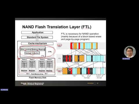
- The flash translation layer, or FTL, maps logical addresses to physical NAND locations because the two address spaces do not correspond directly.
- FTL wear leveling distributes writes across blocks so a single block does not consume its limited program-erase lifetime prematurely.
- FTL garbage collection reclaims blocks, and address mapping lets logically continuous data span multiple physical pages.
- In the lecture's example, a 2 KB page contains 16 kilobits, and a block has 64 rows; NAND programs a page at a time rather than writing arbitrary bytes.
- A sequential write pointer may be at block 2, page 63, so an update to a logical address previously stored at block 0, page 5 must be written to the current physical pointer.
- After the FTL updates the logical-to-physical mapping, the old page becomes invalid garbage, and block valid-page counts must be updated.
- Programming changes selected bits from the erased value of 1 to 0; returning a programmed bit to 1 requires erasing its entire block.
- The program pointer advances page by page through a block and moves to another block at the end, rather than jumping arbitrarily between locations.
- Controller metadata tracks whether a block is erased, how many valid pages it contains, and its erase count to support wear leveling.
- Controllers maintain erased blocks to handle bursts such as saving many phone photos or recording a long video.
- A block with a low share of valid pages, such as 20%, may be selected for reclamation because most of its contents are obsolete.
- Before erasing the block, the controller copies each valid page to the current write pointer; only then can it erase the whole block and restore all bits to 1.
- Adjacent MLC threshold-voltage states use Gray-code-like assignments so neighboring states differ by one bit, limiting a threshold error to one data-bit error.
- TLC encodes 3 bits across 8 levels, while QLC encodes 4 bits across 16 levels; historical usage reserves MLC for 2 bits per cell.
- The overall threshold-voltage window does not expand proportionally with the number of states, so TLC and QLC need tighter distributions and smaller margins, increasing error risk.
- Reading multilevel cells requires several sensing thresholds, often applied sequentially, making MLC, TLC, and QLC reads slower than SLC.
- The threshold shift depends on the amount of charge stored on the floating gate; programming voltage and pulse duration are two ways to control that charge.
- Incremental step pulse programming, or ISPP, applies a program pulse, senses the cell, and gradually raises programming voltage until the target threshold is reached.
- Program-and-verify narrows the threshold distribution and reduces overshoot compared with using one fixed pulse condition.
- Pulse-size choices such as 200 mV versus 500 mV must be characterized for each process and technology node.
- Directly programming an erased cell into one of four MLC states is difficult to control, so foggy programming first creates coarse threshold groups and then refines them.
- Similar staged programming can be used for TLC and QLC, with process-specific protocols rather than one universal method.
- More levels require more program-and-verify iterations; QLC may take over a millisecond to tune its threshold states.
- NAND programming is slow because precise voltage placement takes repeated iterations, while multilevel reads also need multiple sensing cycles.
- Flash reliability centers on endurance, retention, and program/read disturb; endurance measures how many program-erase cycles a cell can tolerate.
- After roughly 10⁵ to 10⁶ cycles in the example, the erased-state threshold rises and the usable memory window shrinks.
- Repeated tunneling damages the tunnel oxide and creates traps that retain electrons, preventing the cell from returning fully to its fresh erased state.
- At elevated temperatures, trapped or floating-gate electrons can escape back toward the channel, reducing stored charge and lowering the programmed threshold voltage.
- Stress-induced leakage current, or SILC, develops through oxide defects created by cycling; traps act as stepping stones that make electron leakage easier.
- Thermal detrapping tends to shift threshold distributions in one direction, while SILC can broaden distribution tails in different directions depending on bias and cell state.
- A retention error occurs when a shifted distribution crosses the reference margin between states, and higher temperature accelerates the degradation.
- Reliability tests bake NAND samples at elevated temperatures such as 200°C, 250°C, and 300°C, then measure time to a defined threshold-voltage failure.
- Plotting log time to failure against inverse thermal energy, 1/kT, produces an Arrhenius relationship whose slope gives the activation energy; the lecture gives about 1.66 eV as an example.
- Thermal energy at 300 K is approximately 0.026 eV, and Celsius measurements must first be converted to Kelvin before calculating 1/kT.
- Accelerated tests let engineers extrapolate from hours or weeks of high-temperature baking toward a commercial target such as 10 years, about 3 × 10⁸ seconds.
- Retention must be measured after cycling as well as on fresh cells: the lecture's projection shifts from about 140°C for fresh material to 114°C after extensive cycling for the same 10-year target.
- Endurance and retention compete: the lecture cites roughly 1,000 program-erase cycles for TLC and QLC, around 10,000 for SLC, and potentially up to 50,000 for SLC.
- During programming, inhibited cells can still experience partial voltage; repeated exposure may shift erased-state thresholds even when the voltage is insufficient to program them fully.
- The word-line pass voltage must balance disturb risks: too high can disturb cells on the selected line, while too low may fail to boost channel voltage adequately in inhibited cells.
- Read operations apply a pass voltage, sometimes around 8 V, to unselected cells; repeated reads can add charge and raise their threshold voltage.
- Read disturb most strongly affects erased cells because their lower threshold leaves a larger effective gate overdrive under the pass voltage.
- More program-erase cycles create more oxide traps, increasing disturb susceptibility and the probability of read errors.
- Erratic overprogramming can occur when trapped holes lower the tunneling barrier, making it easier for electrons to enter the floating gate; distribution-shift patterns help distinguish this from retention loss or disturb.
Transcript excerpt
0:02 Today we will continue our discussions of flash memory. So, let's have a quick recap. We talked about the NOR versus NAND flash. So, here is a simple summary. And if you compare the key metrics between the NOR and NAND, you will find the differences such as the cell size. NOR flash roughly 10 F squared, and then the 2D NAND flash, SLC, I have to mention it's single level cell, is about 4 F squared. Because today we will talk about the multi-level cell, so this will further uh decrease the equivalent cell size for the NAND flash. And then
0:49 the key difference is the random access. So, the NOR flash, you can randomly read from individual locations, but the NAND flash will be very different. We'll talk about that in the next couple of slides. That involve the flash translation layer to map the logical address to the physical address. I'll talk about that in just a couple minutes. And then the program mechanism is different. NOR flash rely on the channel 40 electron, and the NAND flash is F and tunneling. And then the key difference here, the read latency, the NOR is pretty fast. And the NAND is kind of slow. So, with those differences, then in terms of the
1:40 direct comparison here, right? We talked about the mechanism different in terms of the channel 40 electron here versus the F and tunneling. So, the efficiency is pretty low for the channel 40 electrons because you burn a lot of power by passing the current through the mostly through the drain. But only small percentage of the electrons can be redirect to the floating gate. So it's kind of inefficient. And then if you compare the layouts, NAND is more dense, right? So why is that? If you compare just the
This is the start of the transcript. Save this video free for the whole transcript, searchable and time-coded.
Related notes
Summary, takeaways, and chapters were generated by AI from the video's transcript and may contain errors. The video belongs to its creator, Shimeng Yu.