Lecture 2 CMOS Review and Scaling Part 1
 Watch on YouTube →
Overview
Shimeng Yu reviews CMOS transistor operation and explains how subthreshold leakage and short-channel effects constrain voltage and gate-length scaling. He then shows how logic density continues to improve through contact-poly pitch and metal-pitch changes, fin depopulation, design-technology co-optimization (DTCO), and backside power delivery—even though modern process-node labels such as 2 nm no longer correspond to a physical feature size.
Key takeaways
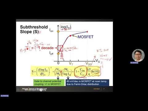
- At 300 K, the ideal MOSFET subthreshold swing is about 60 mV/decade because ln(10)·kT/q is approximately 60 mV; this fundamental limit constrains threshold-voltage and supply-voltage reduction.
- Even picoampere-scale off-state current can create substantial standby power when multiplied across billions of transistors, so reducing Ioff remains essential for battery-powered systems.
- Short-channel effects weaken gate control: a shorter channel or higher drain voltage lowers the source-channel barrier, increasing leakage and causing DIBL.
- Modern logic-node names such as 2 nm and 3 nm do not denote physical gate lengths; CPP, metal pitch, and standard-cell layout are more informative measures of scaling.
- Logic density can improve through DTCO and fin depopulation—for example, replacing three fins with two while maintaining the required drive for a given load.
- Backside VDD/VSS power delivery can reclaim front-side routing space, creating another route to smaller standard cells even after conventional gate-length scaling slows.
Chapters
0:00
Planar NMOS and PMOS Operation in CMOS
- A planar MOSFET is described by its gate, source, drain, channel length, and channel width.
- A positive gate voltage in an NMOS inverts the p-type channel to create an electron-conduction path; PMOS operation uses holes.
- In band diagrams, gate bias lowers the source-to-channel barrier, while drain bias creates a band slope that drives carriers.
6:30
MOSFET Output Curves, Transfer Curves, and Small-Signal Metrics
- The output characteristic plots drain current ID against drain-source voltage VDS at multiple gate-source voltages VGS.
- The transfer characteristic plots ID against VGS and reveals threshold behavior as well as nonzero subthreshold current.
- The linear-region slope relates to channel conductance; the output slope gives output resistance rO, and the change in ID per change in VGS is transconductance gm.
10:50
Why the Room-Temperature Subthreshold Swing Has a 60 mV/Decade Limit
- On a semilog ID–VGS plot, subthreshold current changes approximately exponentially with gate voltage.
- Subthreshold swing is the gate-voltage change required for a tenfold current change; its ideal room-temperature minimum is about 60 mV/decade.
- The limit follows from the MOS capacitor voltage division and Boltzmann carrier statistics: at 300 K, kT/q is about 26 mV, and ln(10)·kT/q is about 60 mV.
18:50
Subthreshold Leakage Sets a Floor for Supply and Threshold Voltage
- Lower supply voltage can reduce dynamic switching energy, which scales approximately with capacitance times voltage squared, but the subthreshold swing limits how far threshold voltage can fall.
- Off current Ioff is nonzero when the gate is at 0 V while the drain remains biased; even picoampere-scale leakage matters across billions of transistors.
- Keeping leakage low requires several decades between off and on current; six decades at 60 mV/decade span 360 mV before adding the overdrive needed for useful drive current.
- The lecture gives practical supply-voltage examples of roughly 500–600 mV at the low end and about 650 mV nominally for a 2 nm process.
25:00
Short-Channel Effects, DIBL, and the On-Current–Leakage Tradeoff
- As the channel shortens, the source-channel barrier falls, increasing the probability that electrons enter the channel even when the gate is off.
- Drain-induced barrier lowering (DIBL) occurs when drain voltage lowers the source-side barrier, shifting threshold voltage and worsening leakage in short-channel devices.
- A well-controlled MOSFET should let the gate dominate channel current rather than allowing drain voltage to control the source barrier.
- High-performance transistor options trade higher Ioff for higher on-current; low-power options sacrifice speed to reduce leakage, with metal-gate work-function engineering used to tune threshold voltage.
33:00
Why Modern 2 nm and 3 nm Logic Nodes Are Not Physical Dimensions
- Technology-node names tracked physical gate length more closely in the 1990s, when labels such as 500 nm and 350 nm aligned with gate dimensions.
- Modern labels such as 5 nm, 3 nm, and 2 nm are technology-generation or marketing identifiers, not measurements of a matching feature on the chip.
- Gate-length scaling has slowed because short-channel effects become harder to control; the lecture cites roughly 15–16 nm gate lengths for recent 2 nm-class devices.
- Logic density can still improve even when gate length barely changes, because layout dimensions and circuit implementation offer additional scaling paths.
37:50
CPP, Metal Pitch, and Fin Depopulation as Logic-Density Levers
- Contacted poly pitch (CPP) measures the distance between adjacent source/drain contact centers and captures more layout area than gate length alone.
- Metal-1 pitch and fin pitch constrain standard-cell dimensions; the lecture gives about 48 nm CPP and 30 nm metal-1 pitch for a 5 nm-class process.
- Fin depopulation can reduce a cell from three fins to two while preserving the drive needed for the same load, increasing density without requiring a faster clock.
- DTCO combines circuit-layout choices with process technology, including tighter spacing and reduced diffusion breaks, to improve cell area within design rules.
43:10
NAND Layout and Intel–TSMC Node-Label Comparisons
- In a two-input NAND layout, series-connected NMOS devices can share an intermediate region without a contact, while parallel PMOS branches require the appropriate contact connections.
- DTCO optimizes transistor spacing and contacts while respecting each process's minimum design rules.
- Intel and TSMC node labels have not been directly comparable: the lecture notes that Intel 10 nm was broadly comparable to TSMC 7 nm, despite the different names.
- CPP and metal-1 pitch provide more useful physical comparisons than node labels alone.
46:15
FinFlex Cells and Backside Power Delivery
- Standard-cell libraries mix different fin counts to balance area and drive strength; a single-fin cell saves area, while higher-performance cells can use more fins.
- TSMC's FinFlex concept allows different fin configurations within a standard-cell library for placement and routing choices.
- Backside power delivery moves VDD and VSS rails behind the silicon, freeing front-side routing space and potentially reducing standard-cell height.
- Yu describes logic-scaling roadmaps as well established for roughly the next decade, with additional gains expected from cell and power-network integration.
49:45
Physical Pitch Definitions in DRAM and NAND Flash
- For DRAM, the traditional 2F definition relates the bit-to-bit distance to a bit-line width plus the spacing between bit lines.
- For 2D NAND, 2F historically corresponds to the poly-gate pitch; in 3D NAND, pitch definitions can instead use the vertical string pitch.
- Memory scaling labels retain closer ties to specific physical pitches than modern logic-node labels.
Summary, takeaways, and chapters were generated by AI from the video's transcript and may contain errors. The video belongs to its creator, Shimeng Yu.