Lecture 5 FLASH Part 2
 Watch on YouTube →
Overview
Shimeng Yu compares NOR and NAND flash architectures, explaining how their cell connections determine density, access patterns, and latency. He details NOR’s channel-hot-electron programming and fast random reads, then NAND’s 4F² cell layout, page and block operations, Fowler–Nordheim tunneling, and channel-inhibition schemes needed to program cells without disturbing their neighbors.
Key takeaways
- NOR’s parallel-cell architecture supports individual random reads at roughly 50 to 100 ns, while NAND’s series strings improve density but can require microseconds for page reads.
- The illustrated cell footprints are about 10F² for NOR and 4F² for planar NAND; NAND approaches the 2F-by-2F minimum by sharing adjacent source/drain regions and eliminating intermediate contacts.
- NOR programs with channel-hot-electron injection using a high drain bias, whereas NAND programs and erases with Fowler–Nordheim tunneling and high gate-to-channel fields.
- NAND programming is page-based and erase is block-based, so rewriting data requires out-of-place updates and a flash translation layer to map logical addresses to physical pages.
- NAND channel self-boosting uses a floating string and capacitive coupling to raise inhibited-cell channel voltage, reducing unintended tunneling during programming.
- NAND read-pass voltage must exceed the highest programmed threshold voltage so unselected cells conduct regardless of their stored state.
Chapters
- Channel-hot-electron programming wastes current because most electrons continue toward the drain instead of reaching the floating gate.
- Split-gate flash separates electron acceleration from vertical injection, using a high drain field to generate energetic electrons and gate coupling to redirect them.
- SST, now part of Microchip, developed SuperFlash IP licensed for embedded flash processes, including 28 nm offerings at foundries such as TSMC and GlobalFoundries.
- Embedded flash stores boot code on-chip in applications such as automotive microcontrollers, where nonvolatile storage must tolerate high temperatures.
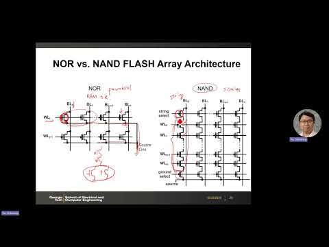
- NOR connects floating-gate transistors in parallel, allowing word-line and bit-line selection of individual cells for reads.
- NAND connects memory transistors in series between string-select and ground-select MOSFETs, so a selected cell’s signal must pass through the rest of its string.
- NAND held over 95% of the standalone flash market in the lecture’s account, primarily because its series architecture enables higher density.
- NOR resembles a DRAM-style individually addressable array, while NAND’s series path makes access less direct.
- Adjacent NOR cells can share a bit-line contact, but high drain voltages of roughly 5 to 8 V require more spacing than a minimum-length logic transistor.
- The illustrated NOR layout is about 10F², approximately 2F by 5F, compared with NAND’s more compact layout.
- NOR programming uses channel-hot-electron injection, while erase uses Fowler–Nordheim tunneling.
- A 2-by-2 NOR array provides a compact example for analyzing erase, program, and read biases.
- NOR block erase applies about 12 V to the common source line and grounds the word lines, causing source-side Fowler–Nordheim tunneling across the block.
- Because Fowler–Nordheim erase current is small, erase can take roughly 100 ms to 1 s.
- To program one cell, the example applies 12 V to its word line, 6 V to its bit line, and grounds the source, producing channel-hot-electron injection in microseconds.
- Inhibit bias prevents other cells from programming: an unselected cell with 0 V at its drain has no substantial current, while a half-selected cell with a low gate voltage remains mostly off.
- NOR read uses about 5 V on the selected word line and 1 V on the drain, enough to sense current without recreating the high-field programming condition.
- A read voltage between the programmed and erased threshold voltages distinguishes high-current and low-current cell states.
- NOR random-read latency is roughly 50 to 100 ns, far faster than NAND’s microsecond-scale page access.
- Repeated programming can shift the threshold voltage of half-selected NOR cells over time, so disturb must be managed even when the initial inhibit bias works.
- A typical two-dimensional NAND string contains 64 floating-gate cells in series, with string-select and ground-select MOSFETs at its ends.
- Adjacent NAND cells share source and drain regions, and intermediate cells need no contact vias because they are not connected externally.
- The resulting 2F-by-2F footprint is about 4F², the theoretical minimum for a planar cell needing word-line and bit-line wiring.
- Both NAND program and erase operations use Fowler–Nordheim tunneling.
- A NAND string’s word lines define pages, while erase operates on an entire block; older examples use 64 cells per string.
- A block can combine 64 word-line pages with thousands of bit-line bytes, producing a highly rectangular array rather than a near-square SRAM or DRAM subarray.
- An older Micron example gives approximately 200 µs for page programming, 500 µs for block erase, and 25 µs for initial page read.
- NAND reads are slow because current may pass through as many as 64 series transistors, accumulating channel resistance and capacitance along the bit-line path.
- NAND erases an entire block at once, while reads and programs operate page by page.
- The erased state is represented as all 1s; programming changes selected bits toward 0, but data cannot be freely rewritten in place.
- When a page needs new data, the controller writes it elsewhere and later erases the old block once its contents are no longer needed.
- This mismatch between logical updates and physical page/block operations requires a flash translation layer to map logical addresses to physical locations.
- NAND block erase applies roughly 20 V to the shared substrate and grounds the word lines, producing Fowler–Nordheim tunneling across the block.
- The ordinary string-select and ground-select MOSFETs cannot tolerate the same high voltage, so their terminals are floated or otherwise protected during erase.
- Programming selects one word line, but the high program voltage also reaches cells on that word line in other strings.
- Unselected cells need an inhibit bias that raises their channel potential, reducing the gate-to-channel voltage below the level needed for significant tunneling.
- In the channel-inhibition example, the selected string receives 0 V on its bit line while other word lines receive a pass voltage, allowing the selected cell’s channel to remain low.
- Turning off the ground-select transistor leaves the string floating, preventing through-current during Fowler–Nordheim programming.
- A floating MOS pass device transfers the lower of its drain voltage and gate voltage minus threshold voltage; for example, a 9 V gate with a 1 V threshold passes at most about 8 V.
- Raising an inhibited cell’s channel to about 8 V reduces a 20 V gate-to-channel bias to roughly 12 V, while the selected cell retains close to the full programming field.
- Modern NAND programming uses channel self-boosting to inhibit unselected strings while keeping select-transistor voltages lower than the earlier 9 to 10 V scheme.
- The sequence first raises word lines to a pass voltage with the string floating, then ramps the selected word line to the program voltage.
- Capacitive coupling from the selected-word-line ramp boosts the floating channel, lowering the electric field across cells that should not be programmed.
- The channel voltage follows a capacitance-divider relationship involving the number of word lines, pass and program voltages, and the cell-to-substrate capacitance ratio.
- Local self-boosting grounds word lines adjacent to the selected row, electrically isolating a smaller channel section so the program voltage contributes more strongly to its boost.
- That local scheme can also cut off the selected programming cell from the bit-line voltage, preventing the desired programming path.
- Asymmetric self-boosting grounds the lower portion of the string while leaving upper cells on pass bias, balancing channel boosting with voltage transfer.
- Asymmetric boosting depends on how many cells lie above the selected word line, so its channel potential varies with the programmed row.
- In the example, erased NAND cells have threshold voltage near −2 V and programmed cells reach about +2 V; a selected-cell read voltage near 0 V distinguishes their states.
- Current from the selected cell must still pass through every unselected cell in the string.
- The read-pass voltage must exceed the highest cell threshold, with about 4 V given as an example, so even programmed cells conduct as pass transistors.
- A small bit-line voltage is sufficient for the sense amplifier to detect whether the selected cell conducts.
- NAND word-line drivers require high-voltage devices and on-chip charge pumps; generating a 20 V word-line level can require pump voltages near 30 V.
- The chip starts from ordinary I/O supplies such as 2.5 or 3.3 V, then uses charge pumps and level shifters to create programming, erase, and pass biases.
- NAND wins standalone-flash density through its compact series layout, but its string architecture makes random reads much slower than NOR.
- NOR remains useful for execute-in-place boot code, where a system can start directly from flash without first copying code into DRAM.
Transcript excerpt
0:02 memory. In last lecture, we talked about the program erase mechanisms and uh we talked about the F internal tunneling and also the channel hot electrons. So, for the channel hot electrons, uh as we mentioned last time, the efficiency is pretty low because you pass a large drain currents but only small probability for the electrons can be redirected to the floating gates. So, then this is uh not very efficient, right? You burn a lot of power essentially, but the the number of electrons that could be injected to the
0:50 bits is very limited. So, the channel hot electron is widely used in the NOR flash. And the for NOR flash, the primary application today is for the on-chip embedded flash. So, this is a special category which we will not spend more time in the rest of the lecture, but here, we just want to briefly mention that. So, for the flash memory, mostly is stand-alone off-chip. It's like DRAM. Mostly it's off-chip. A separate chip. The flash chip. But then for certain applications, you do want the non-volatile memory on-chip. For
1:38 example, for your microcontroller uh to store the initial code you can execute right away when you boot up the system. So, in that scenario, you do need some non-volatile memory on-chip. So, the solution is the eFlash here. And uh embedded flash is co-located with the logic chip. So, it's a very special process flow. So, to enable this e-flash, then this so-called split gate flash is used. It's like 1.5T, 1.5 is like 1/2 transistor structure. So, why is that? So, let's take a look.
2:25 So, this relies on the channel hot electrons. But as we discussed earlier, the efficiency is low. So, here the idea is to split this process into two steps.
This is the start of the transcript. Save this video free for the whole transcript, searchable and time-coded.
Related notes
Summary, takeaways, and chapters were generated by AI from the video's transcript and may contain errors. The video belongs to its creator, Shimeng Yu.