Lecture 1 Overview Part 2
 Watch on YouTube →
Overview
Shimeng Yu surveys SRAM, DRAM, and NAND flash through real processor examples, showing how memory architecture supports CPUs, GPUs, and AI systems. AMD’s Zen 2 and 3D V-Cache illustrate on-chip and stacked SRAM, while DDR5 and HBM3 demonstrate how DRAM packaging and bandwidth address the memory demands of accelerators; NAND scaling and changing memory economics round out the overview.
Key takeaways
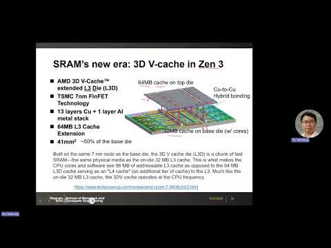
- AMD’s first-generation 3D V-Cache combines a 32 MB L3 cache with a 64 MB stacked SRAM die, providing 96 MB total while requiring software and hardware management of extra access latency.
- SRAM scaling becomes more difficult below 7 nm, so newer AMD cache-stacking designs can keep SRAM on older process nodes while using leading-edge nodes for compute cores.
- DDR5 bandwidth depends on both data rate per pin and pin count: the lecture gives 6.4 Gbit/s per pin and 64 data pins for a typical channel.
- HBM addresses GPU memory bandwidth demands by stacking DRAM dies; the H100 example uses six HBM3 stacks to achieve more than 3 TB/s of aggregate bandwidth.
- Memory technologies serve different roles in modern computing: SRAM supports CPU caches and GPU local storage, HBM feeds high-end GPUs, and NAND provides persistent storage in devices such as smartphones.
- Memory’s economic role is changing: an industry historically focused on lowering cost per capacity now faces AI-driven demand that has made memory more profitable and harder to procure.
Chapters
0:00
AMD Zen 2: Caches and Core-Level SRAM
- AMD’s Zen 2, fabricated on TSMC’s 7 nm process, has four cores and a shared 16 MB L3 cache.
- Each core has private L1 and L2 caches; L1 is split into instruction and data caches.
- Cache arrays contain data and tag regions, alongside peripheral circuitry; cores also include branch prediction and floating-point units.
- The example links AMD’s product turnaround to its TSMC partnership and notes technology metrics including contact poly pitch and standard-cell track count.
5:09
AMD 3D V-Cache and SRAM in Nvidia GPUs
- AMD’s 3D V-Cache stacks a dedicated SRAM die over a compute die using copper-to-copper hybrid bonding.
- The first-generation example combines 32 MB of on-die L3 with a 64 MB SRAM stack for 96 MB of cache; accessing the upper die adds latency.
- Later AMD designs can use older process nodes for SRAM and newer nodes for compute, reflecting the slower scaling of SRAM below 7 nm.
- Nvidia’s A100 example has about 87 MB of SRAM, used across cache, registers, and local scratchpads in its many stream multiprocessors.
11:52
DDR5 DRAM: Density, Data Rates, and Bandwidth
- An SK hynix DDR5 example introduced in 2019 contains 16 Gbit, or 2 GB, of DRAM on a die of about 76 mm².
- DRAM manufacturers often use generation labels such as 1Y instead of disclosing exact process dimensions; the lecture estimates 1Y at roughly 17–18 nm.
- DDR5 data rate is described as up to 6.4 Gbit/s per pin, while bandwidth depends on both per-pin rate and the number of I/O pins.
- A typical DDR channel uses 64 data pins, and banks organize data within the DRAM chip.
15:37
HBM for AI GPUs, NAND Scaling, and Memory Economics
- High Bandwidth Memory stacks DRAM dies vertically using advanced packaging, microbumps, and through-silicon vias; stacks can reach 12 or 16 dies.
- The Nvidia H100 example pairs a roughly 800 mm² TSMC 5 nm GPU die with six HBM3 stacks and more than 3 TB/s of aggregate bandwidth.
- Two-dimensional NAND scaling reduced die area for a fixed 128 Gbit capacity by an average of about 28% per generation before the shift toward 3D NAND after 2015.
- The lecture connects NAND to smartphone storage, HBM to AI GPUs, and SRAM to CPUs, while noting that memory has shifted from a cost-driven market toward high demand and profitability.
Summary, takeaways, and chapters were generated by AI from the video's transcript and may contain errors. The video belongs to its creator, Shimeng Yu.