Lecture 9 RRAM
Overview
Shimeng Yu explains oxygen-vacancy RRAM and conductive-bridge CBRAM, then focuses on hafnium-oxide RRAM: its switching physics, variability, reliability tests, and array integration. Drawing on ITRI and IMEC research and later chip demonstrations, he traces commercialization from early prototypes to embedded RRAM in TSMC’s 12 nm FinFET process, positioning it as a candidate to replace embedded flash in microcontrollers.
Key takeaways
- Hafnium-oxide RRAM stores data through a localized oxygen-vacancy filament, and a capping layer acts as an oxygen reservoir that enables reversible set and reset.
- Filament formation is inherently variable: vacancy positions and filament shapes change across devices and cycles, motivating write-verify programming and error-correcting codes.
- Retention claims require failure measurements at multiple temperatures and Arrhenius extrapolation; a short bake followed by a simple projection cannot reliably establish 10-year data retention.
- Multilevel RRAM can encode two bits using four resistance states, but write-verify programming can increase latency from 8 ns to about 160 ns in a demonstrated chip.
- RRAM’s strongest commercialization case is embedded memory: TSMC’s 12 nm FinFET integration targets MCU applications beyond embedded flash’s approximate 28 nm scaling limit.
Chapters
- Shimeng Yu distinguishes oxygen-vacancy RRAM, often called oxide RRAM, from metal-ion CBRAM, which forms a conductive bridge from copper or silver.
- In oxide RRAM, a metal-oxide layer sits between two electrodes; oxygen vacancies form a conductive filament that switches the device from high resistance to low resistance.
- A compliance current, such as 100 microamps, limits current during set to reduce the risk of device breakdown; reversing voltage resets the device.
- CBRAM uses oxidation, ion migration, and reduction to deposit metal atoms into a bridge, but fast copper or silver diffusion creates fabrication concerns.
- Research reported switching in oxides made from many periodic-table elements, but industry emphasized fab-compatible materials such as hafnium, zirconium, tantalum, and aluminum oxides.
- Representative RRAM metrics include roughly 10 ns read/write, programming voltages of 1 to 3 V, and programming currents up to 100 microamps.
- Reported endurance spans 1 million to 1 trillion cycles, while a typical retention target is 10 years at 85°C.
- Atomic layer deposition below 300°C supports back-end-of-line integration above CMOS transistors and interconnects.
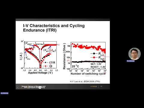
- ITRI’s 2008 device combined a 30 nm hafnium-oxide RRAM cell with a 180 nm access transistor in a 1T1R structure.
- The hafnium oxide was intentionally oxygen-deficient, and a titanium capping layer scavenged oxygen to promote vacancy formation.
- The reported device retained a resistance window through 10^6 switching cycles, although its high-resistance state degraded over cycling.
- Pulse testing reported switching with 300 ps pulses, with faster operation requiring increased voltage; retention projections based only on a short bake were considered overly optimistic.
- IMEC’s 2011 IEDM work demonstrated a 10 nm by 10 nm active RRAM area controlled by a substantially larger 65 nm access transistor.
- The hafnium capping layer, like ITRI’s titanium layer, scavenged oxygen from hafnium oxide to create vacancies.
- Initial electroforming required higher voltage than later set/reset cycles; a 10 nm cell with 5 nm oxide could require about 2.5 V to form, compared with roughly 1 V afterward.
- Forming voltage depended on cell area and capping-layer thickness, while later switching data supported the view that only a localized filament conducts.
- IMEC found that endurance failure depended on set strength, controlled through the access transistor’s word-line voltage and resulting compliance current.
- A weak set could leave the cell stuck in the high-resistance state; an overly strong set could leave it stuck in the low-resistance state.
- Optimizing set and reset pulse amplitudes and widths balanced the two failure modes and enabled a reported endurance of 10^10 cycles.
- A reliable retention projection records time to failure at multiple temperatures, then uses an Arrhenius plot of log time to failure against 1/kT.
- IMEC measured resistance degradation at 150°C, 200°C, and 250°C; the reported activation energy was about 1.2 to 1.5 eV.
- Multilevel cell states can be created by stopping reset at different voltages or applying different set compliance currents.
- Four resistance levels can encode two bits, but retention of each level needs rigorous testing rather than simple extrapolation.
- Shimeng Yu describes forming as a breakdown-like event in which a strong electric field moves oxygen ions out of the oxide lattice and leaves an oxygen-vacancy filament.
- The capping layer acts as an oxygen reservoir, preserving oxygen near the interface so reverse bias can return oxygen ions and rupture the filament.
- Because filament shape and vacancy location vary from cycle to cycle, RRAM exhibits both device-to-device and cycle-to-cycle variability.
- Yu’s PhD work used kinetic Monte Carlo simulation to track oxygen motion and coupled it with electron tunneling to reproduce measured current-voltage behavior.
- IMEC researchers used conductive atomic force microscopy after removing an electrode to map current through the exposed hafnium-oxide surface.
- The fresh device showed low current, set produced a localized high-current filament under 50 nm wide, and reset largely removed its conductive signature.
- Cross-sectional TEM with electron energy-loss spectroscopy showed reduced oxygen concentration in the filament region and oxygen transfer toward the capping layer.
- The side-view measurements estimated a filament around 15 nm wide, supporting a localized rather than whole-device switching mechanism.
- Oxygen vacancies create electronic trap states in the oxide, allowing electrons to conduct through trap-assisted tunneling rather than direct tunneling across the 5 to 10 nm film.
- A later Italian research group extended earlier two-dimensional simulations to a three-dimensional model of oxygen and vacancy movement.
- The simulations connect filament growth during forming or set with changes in measured current.
- ITRI’s 2011 prototype was a 4 Mbit 1T1R chip in 0.18-micron CMOS, with 30 nm by 30 nm RRAM cells.
- The chip demonstrated two-bit operation using four resistance distributions; write-verify pulses reduced distribution overlap and improved sensing margin.
- Write-verify increased two-bit programming time to about 160 ns, compared with 8 ns for one-bit programming.
- Panasonic reported an 8 Mbit cross-point 1S1R array with a bidirectional selector and 17 ns parallel programming for one-bit operation.
- Panasonic announced an RRAM-equipped microcontroller in 2013, following its earlier array demonstration.
- SanDisk and Toshiba reported a 32 Gbit, two-layer 1S1R chip using 24 nm technology, while Sony and Micron demonstrated a 16 Gbit CBRAM chip using copper and 27 nm technology.
- The large-capacity chip reports listed microsecond-scale latency, slower than the tens-to-hundreds of nanoseconds reported for smaller prototypes.
- After limited announcements from 2014 to 2018, standalone-memory development quieted before logic foundries revived interest in embedded RRAM.
- TSMC announced embedded RRAM in its 14 nm process in 2018, targeting replacement of embedded flash rather than standalone memory.
- Intel reported a 10 Mbit/mm² RRAM implementation in a 22 nm FinFET process in 2019, with the memory integrated in the metal stack.
- The embedded RRAM cells were not exceptionally small because the relatively high programming current required larger access transistors.
- Forming voltage could require an I/O transistor, while reported switching speeds were generally below 10 ns and endurance was around 10^3 to 10^4 cycles.
- TSMC progressed its embedded RRAM from 40 nm and 22 nm offerings toward 12 nm FinFET integration, including a 2024 demonstration.
- The opportunity is tied to embedded flash scaling: Yu notes that embedded flash is limited to about 28 nm, while RRAM can support more advanced MCU processes.
- The 12 nm implementation places 1T1R cells between metal 4 and metal 5 and uses error-correcting codes to address cell variation.
- TSMC reported volume production and rising customer demand; Yu also recounts a tape-out shuttle being postponed because customer designs had priority.
- Automotive microcontrollers are an important embedded-RRAM market because they need nonvolatile memory for functions such as boot-up and must meet high-temperature qualification requirements.
- Yu cites Infineon as a major MCU producer using RRAM in automotive products and notes industry hiring demand for engineers with RRAM design and tape-out experience.
- The shift from research prototypes to foundry production and automotive customers marks RRAM’s move toward practical embedded-memory deployment.
Transcript excerpt
0:03 which is one of the emerging non-volatile memory. So we already talk about the principle of those emerging non-volatile memories and today we will dive deep into the resistive random access memory RRAM. So actually I had a long history with this technology because when I was doing my PhD I mean almost 18 years ago my research topic was on RRAM. And I spent quite some time especially in my early career working on this technology.
0:50 So yeah I made some fundamental contributions to the technology from the physical mechanisms to the device modeling to the chip level implementations of the RRAM technology. So I will share some of my learnings and experiences doing this research with you today. So first of all some high-level introduction of the RRAM technology and then we will go over some representative device uh characteristics from the data reported by two research institutions. One is called ITRI in Taiwan
1:37 and the other one is IMEC in Europe. And then we will discuss the physical mechanisms of the RRAM's operation and finally we will show you some array level integration and the prototype chip demonstrations. And finally I will talk about the commercialization of this technology where the technology stands in the today, okay? So RRAM, resistive random access memory and actually it can be classified into two sub category. So here you see on the left we have the oxygen vacancy based RRAM or sometimes people call it ox run because it's based on oxide.
2:26 So here the device structure is simple, it's a two terminal device. You have two electrode and then in the middle you have some oxide thin film, metal oxide thin film. And the mechanism as we discussed before is to create this filament of the oxygen vacancy. So electrons can
This is the start of the transcript. Save this video free for the whole transcript, searchable and time-coded.
In this course
Related notes
Summary, takeaways, and chapters were generated by AI from the video's transcript and may contain errors. The video belongs to its creator, Shimeng Yu.