Lecture 6 Emerging Memories Part 1
Overview
Shimeng Yu surveys emerging nonvolatile memories, explaining how MRAM, phase-change memory (PCM), resistive RAM (RRAM), and ferroelectric memories encode data using magnetic orientation, atomic structure, resistance, or polarization. He compares their trade-offs and market niches, then develops the array-design challenges of 1T1R and 1S1R crosspoint architectures, including programming current, sneak paths, write-disturb biasing, sensing, selector nonlinearity, and interconnect IR drop.
Key takeaways
- Emerging memories are not universal replacements: MRAM, PCM, RRAM, and ferroelectric cells occupy different niches because their speed, density, endurance, voltage, and write-current trade-offs differ.
- In a 1T1R array, programming current can force an access transistor to grow well beyond minimum size; a 28 nm minimum transistor may deliver only about 10 to 15 microamps, while some memory writes need hundreds of microamps or more.
- A 1S1R crosspoint array can target a 4F² cell, but it depends on a two-terminal selector to suppress sneak paths through unselected cells.
- Crosspoint write schemes trade disturb protection against power and bias exposure: V/3 limits unselected-cell stress to one-third of the write voltage, but biases more cells than V/2.
- Selector nonlinearity is central to crosspoint readability: a ratio of 10 to 20 between full-bias and half-bias currents suppresses leakage far more effectively than the ratio of about 2 from a linear resistor.
- MRAM's roughly 2:1 resistance ratio makes it less suitable for selector-based crosspoint arrays than RRAM or PCM devices that can exhibit ratios of 10 to 100.
Chapters
- SRAM serves on-chip caches, DRAM serves main memory, and NAND flash provides long-term storage.
- No universal memory combines SRAM-like speed with flash-like density, so the hierarchy leaves latency and capacity gaps.
- Emerging technologies are evaluated as possible ways to fill those gaps rather than as automatic replacements for established memories.
- An ideal memory would combine nonvolatility, high density, low power, random access, fast operation, endurance, scalability, and CMOS compatibility.
- SRAM, DRAM, and flash store information through charge, using capacitors, parasitic capacitance, floating gates, or charge traps.
- Many emerging memories instead change atomic configurations or other physical properties, reducing reliance on shrinking quantities of stored charge.
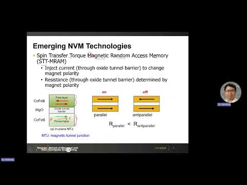
- Spin-transfer-torque MRAM uses a magnetic tunnel junction with a fixed pinned layer, a switchable free layer, and a thin MgO tunnel barrier.
- Parallel magnetization produces lower resistance than the antiparallel state, allowing a sense amplifier to distinguish the two bit values.
- MRAM stores information in magnetic orientation rather than charge, with resistance providing the readout.
- Phase-change memory commonly uses chalcogenide compounds such as Ge₂Sb₂Te₅, whose crystalline and amorphous phases have different resistance.
- The crystalline phase is lower resistance; the amorphous phase is higher resistance because its atoms lack long-range order.
- Heating and rapid quenching can freeze a disordered amorphous state, while controlled heating can restore the crystalline state.
- RRAM typically uses a thin metal-oxide layer between two electrodes, with switching driven by oxygen-vacancy formation and movement.
- A conductive filament bridges the electrodes to create a low-resistance state; reversing or removing the applied voltage can rupture the path.
- The filament's formation and rupture provide the resistance change used to represent data.
- In the examples compared, the low-resistance state represents 1: parallel magnets in MRAM, crystalline PCM, and a formed RRAM filament.
- PCM can use unipolar switching, where set and reset use the same voltage polarity but different amplitudes.
- Typical RRAM and STT-MRAM switching is bipolar: set and reset require opposite voltage polarities.
- Ferroelectric crystals can retain polarization in either direction, creating distinguishable states through aligned dipoles and surface charge.
- A ferroelectric field-effect transistor, or FeFET, uses polarization to shift transistor threshold voltage, somewhat like charge storage shifts the threshold in flash.
- FeRAM combines a transistor with a ferroelectric capacitor; sensing polarization reversal can produce a detectable transient current.
- MRAM offers low-voltage operation and strong endurance, but its write time remains slower than SRAM and its resistance-state margin can be limited.
- FeFET can offer lower write voltage and faster operation than NAND flash, but it does not match modern 3D NAND density.
- MRAM and RRAM are used in automotive and industrial microcontrollers, where SRAM can face high-temperature leakage or radiation-induced soft errors.
- Emerging memories do not replace cache or NAND wholesale; their value depends on matching their speed, density, endurance, and operating conditions to a specific tier.
- Yu contrasts emerging-memory prototypes with NAND, DRAM, and SRAM, noting that the figures shown are historical and some need updating.
- The lecture cites 3D XPoint at about 600 Mb/mm² at its announcement, compared with roughly 80 Mb/mm² for the DRAM generation discussed.
- For bandwidth, DRAM technologies such as HBM and GDDR remain strong because memory interface design also determines achievable throughput.
- A 1T1R cell places a variable resistor under the control of an access transistor, in an arrangement analogous to DRAM's 1T1C cell.
- A tightly optimized layout could approach 6F², but practical spacing and transistor sizing can push cells beyond 12F², potentially to 20F² or 40F².
- RRAM, PCM, and MRAM programming can require hundreds of microamps or more, while a minimum transistor at a 28 nm node may supply only about 10 to 15 microamps.
- A crosspoint array replaces each access transistor with a two-terminal selector in series with a variable resistor, forming a 1S1R cell.
- Two perpendicular wires define each cell, enabling a nominal 4F² footprint and making the architecture attractive for PCM and RRAM.
- Without selectors, current can flow through unselected resistors as sneak paths, obscuring the selected cell's signal.
- MRAM is a difficult crosspoint candidate because its on/off resistance ratio is about 2, compared with roughly 10 to 100 for some RRAM and PCM devices.
- In a bipolar crosspoint array, the selected word and bit lines receive opposite biases for set or reset, placing the full write voltage across the target cell.
- V/2 biasing applies half the write voltage to cells sharing the selected row or column, while other cells ideally see zero voltage.
- V/3 biasing reduces the maximum voltage across an unselected cell from V/2 to V/3, lowering disturb risk.
- V/3 exposes more unselected cells to a partial bias and can consume more power; row programming may also require separate set and reset passes for mixed data.
- Current sensing applies a small read voltage and measures the selected cell's current, which depends on whether its resistance is high or low.
- Voltage sensing precharges a bit line and observes its discharge rate, using the resistance-dependent decay in a manner similar to SRAM or DRAM sensing.
- Unselected rows must be biased to prevent their cells from contributing unwanted current or voltage decay.
- A crosspoint selector must be a two-terminal switch, rather than a three-terminal transistor, to preserve the compact 4F² layout.
- The desired bidirectional behavior is low leakage below a threshold and strong conduction above it, for both positive and negative voltages.
- In a 1S1R stack, the selector suppresses low-voltage current while allowing the resistance states to remain distinguishable during reads.
- A selector's nonlinearity ratio compares current at the full write voltage with current at half that voltage.
- A linear resistor gives a ratio of about 2 under half-voltage bias, while useful selectors can reach ratios of 10 to 20 or higher.
- Reported selector behaviors include gradual exponential current-voltage curves and sharper threshold switching; both aim to reduce sneak-path current.
- The lecture closes by noting that selector designs remain an active research area and continues the topic in the next lecture.
Transcript excerpt
0:06 So today we will have a new section on the emerging native memory. So we will discuss a few emerging nominal time memory candidates uh at a high level because in the following lectures we will have individual sections on each of those emerging native memory technology one by one. So today we will have some high level discussions and then we will talk about some generic array architectures to support those emerging number memory and especially we'll discuss some design considerations including the selector device and the
0:56 interconnect and uh probably next lecture we will discuss one example that is 3D exponent memory which was commercialized earlier by Intel and Micron. So you are familiar with this memory hierarchy. We discussed that at the very beginning of the semester and we already have gone through the mainstream technologies one by one. Right? So s D run flash non flash and you know the role of those each memory is to serve the different levels in this hierarchy srun as you know on chip cache L1 L2 L3 D run the main memory
1:48 typically off chip those SRA and D RMS are volatile 12 once you turn off the power supply then you lose the data. So for longterm storage n flash is a mainstream technology today for the SSD and so on. So the reason we have this memory hierarchy as we discussed before is that because there's no universal memory that you can have both fast speed that means small latency and simultaneously have large capacity or highest density. So we have the trade-offs that's why we have the hierarchy. But of course you
2:36 can say that between the levels there's a gap in terms of in terms of the latency and capacity. Then that rais the question would there be opportunity
This is the start of the transcript. Save this video free for the whole transcript, searchable and time-coded.
In this course
Related notes
Summary, takeaways, and chapters were generated by AI from the video's transcript and may contain errors. The video belongs to its creator, Shimeng Yu.