Lecture 8 Array and Bank-level Design
Overview
Michael Carr explains how memory arrays scale from cells and mats into banks, caches, and full memory systems, linking organization choices to latency, bandwidth, area, and energy. He compares decoder and driver designs, bitline and sense-amplifier multiplexing, and voltage- versus current-mode sensing, then applies those trade-offs to SRAM, resistive memories, and cache layouts. The lecture closes with CACTI and related tools for exploring memory power, performance, and area across design parameters.
Key takeaways
- Banking increases potential parallelism but is not true multiporting: two requests that map to the same bank must be serialized.
- Predecoding reduces decoder complexity and fan-out; the 45 nm NCSU PDK example cuts the implementation from 136 CMOS gates to 104.
- Latch-based SRAM sense amplifiers retain read data for reuse, while current-mirror designs avoid storing the internal result but require inverter restoration.
- Fine-grained cache partitioning improves access speed and attainable bandwidth at the cost of area, wire length, and energy per bit.
- Repeaters can shorten global-wire delay but cannot remove the energy consumed charging parasitic wire capacitance.
- Memory design tools such as CACTI make it practical to explore architectural and circuit trade-offs across capacity, associativity, timing mode, and optimization targets.
Chapters
- Michael Carr introduces array design as a practical guide to peripheral circuits and memory-organization choices, with relevance to circuit labs.
- A RAM interface uses physical addresses, write data, read data, commands, and sometimes status outputs such as cache-tag results.
- Multiple ports enable simultaneous independent accesses, as in register files; banking allows parallel requests only when they map to different banks.
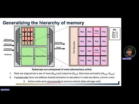
- Banks or slices operate as independent functional units, while an interconnection network routes requests from cores to them.
- Active subarrays contribute portions of a requested block; in the example, a 16 KB bank block divided across four active subarrays yields 4 KB per subarray.
- Mats form the lowest-level array units, with row and column activation allowing multiple mats to contribute data in parallel.
- Selecting one of M word lines requires log₂(M) address bits and an injective mapping from each address to one activated line.
- A conventional n-input decoder uses roughly 2ⁿ AND gates plus input inverters; static pseudo-NMOS saves transistors but draws static current.
- Dynamic NOR logic precharges an internal node and evaluates it through an NMOS pull-down network, trading low static power for higher dynamic power.
- Using a 45 nm NCSU PDK example, pairwise predecoding reduces a decoder implementation from 136 CMOS gates to 104 and lowers fan-out.
- Decoder outputs drive large word-line capacitances from many cell gates and long wires, so additional driver stages are often needed.
- A latency-optimized chain sizes stages using logical and electrical effort, commonly targeting a fan-out near four, but uses the most area.
- An area-optimized two-stage design sizes its final stage for current requirements and reduces area at the cost of higher delay.
- A balanced design combines output-current sizing with effort-based sizing for earlier stages, moderating both delay and area.
- Bitline multiplexers sit between arrays and sense amplifiers and use pass gates or transmission gates to preserve low-swing analog signals.
- Sharing sense amplifiers through bitline multiplexing can reduce circuit area, but the added resistance and parasitics affect the signal path.
- DRAM generally cannot use this form of bitline multiplexing because every activated cell must be restored by its sense amplifier.
- Sense-amplifier multiplexers select among latched row-buffer data digitally, helping reuse fetched data when the number of output I/Os is limited.
- Carr models the bitline as a distributed RC path, the cell as a Norton current source with output resistance, and the amplifier input as a load resistance.
- Voltage sensing favors a high input resistance to limit divider loading; current sensing favors a low-resistance path for the sensed current.
- The idealized timing comparison predicts faster current sensing, although its advantage narrows as bitline wire resistance increases.
- Current sensing adds circuit complexity, so array size and implementation costs can change which sensing mode is preferable.
- An SRAM latch-based sense amplifier precharges both bitlines to 1 V, develops a differential during word-line activation, then latches the result when sense enable is asserted.
- The illustrated SRAM cell develops its sensing margin in about 160 ps; a current-mirror voltage-mode amplifier instead produces a smaller differential that an inverter restores.
- Latch-based amplifiers retain data for row-buffer reuse and have lower static power, while current-mirror designs follow the signal but need an output inverter and do not retain the value.
- For ReRAM, MRAM, and phase-change memory, voltage-mode sensing compares the cell trajectory against a reference voltage; current-mode sensing compares read current with a dummy-array reference current.
- Local sensing places amplifiers near individual mats and carries full-swing digital signals across the hierarchy; global sharing can amortize amplifier area but uses partial-swing analog paths.
- Destructive DRAM reads constrain amplifier sharing because the sense amplifier must restore the cell state locally.
- Uniform cache access equalizes bank latency, while non-uniform cache access makes latency depend on bank proximity and network hops.
- The Sun Niagara example uses distributed cache banks connected by a large crossbar; AMD Zen 3 3D V-Cache combines adjacent slices, a bidirectional ring, and paired slices connected through TSVs.
- More partitioning can increase access speed and bandwidth, but generally costs area, routing length, and energy per bit; fewer partitions favor area efficiency and shorter routes.
- Repeaters can reduce the delay of a 1 mm full-swing global wire, but cannot eliminate the energy cost of its parasitic capacitance.
- Caches use relatively fine-grained arrays, while DRAM mats can contain thousands of rows and columns; the difference reflects their distinct speed requirements.
- Total transaction latency is not the same as critical-path latency: pipelining can sustain repeated mat accesses, but a slow mat limits maximum bandwidth.
- Larger blocks can raise theoretical bandwidth, but retrieving unnecessary data can waste energy and pollute a cache.
- CACTI models memory power, performance, and area using RC networks and timing models, enabling bank-level exploration without building every design in SPICE.
- Related tools extend the design space: NVSim covers emerging nonvolatile memories and crossbars, while DESTINY adds 3D-cache and updated eDRAM modeling.
- The lab's compute-in-memory modeling work and newer NeuroSim-related tooling support additional memory technologies and integration options, including FinFETs, nanosheets, oxide-semiconductor devices, and gain cells.
- Lab 5 uses parametric exploration of capacity, associativity, timing mode, and memory type to compare designs optimized for area, leakage, or speed.
Transcript excerpt
0:00 My name is Michael Carr. I'm a PhD student in Dr. Shimon Yuslab. And today I'm going to talk about array design. Um, in previous years, this has been a two-part series. Uh, in this particular series, we're going to condense it into a single part. Um, and so it will be a little bit accelerated. Sorry about that. Uh, it will be a little bit accelerated. Um but hopefully this will be uh quite useful for things like the labs and also a high level understanding of how we actually make design decisions uh when constructing memory arrays. Until now uh we focus pretty much entirely within the scope of how memory cells are interconnected. uh and though we might have focused some of our
0:47 discussions on uh how you know creating rows and columns of these and these are exercis these memory cells might be exercised with uh perfect voltages or perceived currents. Uh we haven't really discussed how exactly the peripherals on these outer boundaries work and one thing we also haven't discussed a whole lot is how exactly we partition or use arrays. what sort of array sizes are useful to us and what are the trade-offs when constructing something larger like a full cache memory or full bank. Uh and so we're going to focus on those two things. We're also going to spend some time communicating some of the trade-offs uh between different sense amplifier designs with a more rigorous focus. Um the reason for this is lab 4 will focus on sunsamplifier designs uh and actually running those in spice. So
1:35 this will hopefully be useful. We're going to start by going from the top downwards. Uh what I've depicted here is a die photo, a high quality die photo from the photographer friction
This is the start of the transcript. Save this video free for the whole transcript, searchable and time-coded.
In this course
Related notes
Summary, takeaways, and chapters were generated by AI from the video's transcript and may contain errors. The video belongs to its creator, Shimeng Yu.