Lecture 9: CMOS Inverter - Part 2
 Watch on YouTube →
Overview
The lecture explains how CMOS inverter gain creates regenerative logic: degraded signals are restored toward 0 and VDD, enabling noise-tolerant logic chains and stable SRAM states. It then connects inverter behavior to leakage and switching power, fan-out, short-circuit current, supply-voltage trade-offs, and odd-stage ring oscillators used to measure propagation delay.
Key takeaways
- A high-gain CMOS inverter restores degraded logic levels toward 0 and VDD, provided the input has not crossed the logic threshold.
- Cross-coupled inverters have two stable complementary states that store an SRAM bit; the intermediate VDD/2 state is metastable and vulnerable to noise.
- Wider butterfly-curve lobes indicate greater resistance to memory bit flips because a larger disturbance is needed to move the cell out of a stable state.
- Dynamic power increases with switching frequency, supply voltage, and load capacitance, while fan-out optimization can reduce the capacitance seen by a gate.
- Lowering VDD reduces dynamic energy but increases delay and can increase leakage energy, so total energy has an optimum supply voltage rather than improving indefinitely.
- An odd-stage ring oscillator oscillates with period approximately 2Ntp, providing a practical method to estimate inverter propagation delay.
Chapters
- A steep CMOS inverter voltage transfer characteristic (VTC) provides higher gain and noise margin, improving immunity to input noise.
- During a low-to-high or high-to-low transition, NMOS and PMOS can conduct simultaneously, creating a temporary current path from VDD to ground.
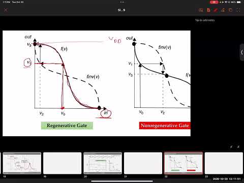
- Regenerative behavior is introduced as a core property shared by inverter chains and other digital logic gates.
- A butterfly curve overlays an inverter VTC with its reflection, representing alternating stages in an identical inverter chain.
- For a 5 V supply, an imperfect 3 V input is treated as logic high because it is above the approximate 2.5 V logic threshold.
- Tracing successive VTCs shows a degraded input moving closer to the rails, with later stages approaching VDD and 0.
- Restoration works only while degraded signals remain on the correct side of the logic threshold; crossing it can cause a logic error.
- A VTC with insufficient gain can leave a signal oscillating around intermediate voltages instead of restoring it to 0 or VDD.
- High inverter gain supports both noise margin and regeneration by pushing signals toward stable logic levels.
- The shape of the butterfly curve can reveal whether a logic technology is likely to recover degraded signals.
- Load-line analysis finds a system solution where two device responses intersect, satisfying a shared current or voltage condition.
- In cross-coupled inverters, each inverter's output feeds the other's input, so their VTCs intersect at possible steady-state voltages.
- The system has two rail-level stable states and a third intermediate metastable point.
- The two stable states are complementary node values: one node is near 0 while the other is near VDD, or vice versa.
- An SRAM cell uses cross-coupled inverters to reinforce and retain either stored state.
- Access transistors connect external data to the internal nodes during writing, forcing the cell from one stable state to the other.
- A balanced cross-coupled pair can sit temporarily near VDD/2, but that operating point is metastable rather than robust.
- Thermal noise, characterized in part by kT/q, can nudge the node slightly left or right of the intermediate point.
- Regenerative feedback amplifies that small perturbation until the circuit settles into one of its two stable rail-level states.
- Digital gates tolerate bounded disturbances because regeneration returns signals toward 0 or VDD; analog circuits instead respond to small signal changes.
- Wider lobes in a butterfly curve indicate greater stability for stored data, since larger disturbances are needed to flip a bit.
- Higher gain supports larger noise margins and wider memory-stability lobes, although a stable state can also be harder to switch deliberately.
- Static power is consumed even when a logic gate is idle because transistor leakage continues over time.
- The lecture distinguishes gate leakage through the gate structure from junction leakage associated with source and drain regions.
- Leakage power depends on voltage and aggregate leakage current, making small per-device currents significant across large transistor counts.
- A CMOS output alternately charges through the PMOS network and discharges through the NMOS network.
- The output load can be modeled as a capacitor charged and discharged through transistor resistance.
- Dynamic switching power rises with switching frequency, supply voltage, and load capacitance; reducing VDD or frequency lowers this component.
- Downstream transistor gates contribute input capacitance to the driving gate's load.
- Driving five gate inputs adds roughly five gate-capacitance loads, increasing switching demand and potentially slowing the output.
- Fan-out optimization distributes branches across logic nodes to balance load, speed, and power.
- Short-circuit current occurs during input rise and fall times, when both NMOS and PMOS devices can conduct together.
- Unlike load-capacitance charging and discharging, this power is concentrated at signal transitions rather than stable logic levels.
- Longer rise and fall times increase short-circuit power, so faster transitions reduce the time spent in the overlap-conduction region.
- Lowering VDD reduces dynamic energy, but it also increases circuit delay.
- Leakage energy can rise at low VDD because delay grows sharply while leakage power falls less rapidly.
- Total energy therefore has an optimum supply voltage; reducing VDD indefinitely is not necessarily the most efficient design choice.
- Steeper-switching transistors can shift the energy minimum toward a lower VDD.
- Comparing VTCs at different supply voltages shows that the curve's endpoints move inward as VDD decreases.
- Inverter gain can improve over part of the lower-voltage range, but at sufficiently low VDD the VTC loses gain.
- Once gain is inadequate, regeneration and noise immunity weaken, so designers must evaluate VDD against power, delay, and logic reliability.
- A ring oscillator connects a chain's final inverter output back to its input; an odd number of stages prevents a static logic assignment and produces oscillation.
- For N inverter stages with per-stage propagation delay tp, the oscillation period is approximately 2Ntp.
- Measuring the period with an oscilloscope allows tp to be estimated without measuring an individual inverter directly.
- A 99-stage ring oscillator is described as a standard way for foundries such as TSMC, Samsung, Intel, and GlobalFoundries to compare transistor speed.
Transcript excerpt
0:02 Okay. So, here it goes. We have been discussing CMOS inverter and we have reached up to this point where we discussed uh the concept of noise margin and gain. Okay? So, the steeper the transition at the CMOS inverter, the better it is in terms of gain and performance because it gives you the higher noise margin. Quick question, do you like high noise margin or low noise margin again? High. Okay? Because that gives you immunity uh with respect to noise. We also discussed the concept of short-circuit current. Whenever there is a transition from high to low or low to high, you have a overshoot of current because the NMOS and PMOS transistors
0:49 both turn on momentarily at the same time and they have some kind of a short circuit between VDD and ground. And that leads to significant current surge, which is not good uh as you can imagine. All right. Now, this is where we begin today, regenerative property. And I told you before that this is this uh lecture is foundational to the next one. I've already uploaded the slides for the next lecture. You can see that. Uh this is basically uh about digital logic design in general. And all digital circuits that you ever learn about will have the same properties that we are discussing here. Regenerative property is one of them. And what is that? So, imagine you have a chain of inverter. So, one inverter driving another, driving another, driving another. But I would say, instead of considering it as a chain of inverter, think of it like a chain of digital
1:38 logic circuit. Okay? Because it doesn't matter which kind of If it is a NAND gate, NOR gate, XOR gate, it's all the same. The concept that I'm going to talk about now is
This is the start of the transcript. Save this video free for the whole transcript, searchable and time-coded.
Related notes
Summary, takeaways, and chapters were generated by AI from the video's transcript and may contain errors. The video belongs to its creator, NorDIC Lab.