Lecture 2: MOSFETS & FinFETs - A Quick Overview (Part 2)
 Watch on YouTube →
Overview
The lecture builds from silicon band gaps and donor/acceptor doping to explain how an NPN MOSFET controls electron flow through energy barriers. It connects source-to-drain band diagrams, Fermi-level alignment, drain-induced barrier lowering (DIBL), and the vertical MOS capacitor structure, showing how gate voltage bends silicon bands to create an inversion layer.
Key takeaways
- Donor doping creates an energy level near silicon's conduction band, allowing dopant electrons to become mobile without the paired hole produced by intrinsic electron-hole generation.
- An NPN MOSFET's source and drain are heavily doped N+ to reduce resistance, while its p-type body creates an energy barrier that controls source-to-drain electron flow.
- VDS creates an energetic preference for electrons to reach the drain, but VGS must lower the source-side barrier for substantial current to flow.
- DIBL is a short-channel effect in which drain voltage lowers the source barrier, increasing off-state leakage and potentially enabling unwanted conduction.
- Positive gate voltage on a p-type MOS structure first depletes holes and then attracts minority electrons, creating an inversion layer that behaves like an n-type channel.
- The MOSFET gate and silicon surface form a capacitor separated by oxide, so charging and discharging gate capacitance constrains circuit switching speed.
Chapters
- A semiconductor has a valence band and conduction band separated by a forbidden band gap; insulators generally have a wider gap.
- The familiar lines in a band diagram mark band edges, not the full bands, which extend beyond the illustrated energy range.
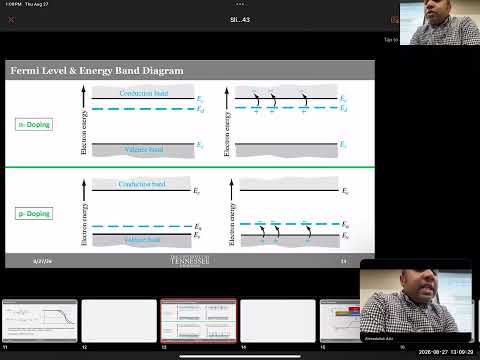
- Donor doping introduces an energy level near silicon's conduction band, allowing electrons to become mobile with less energy than a valence-to-conduction transition requires.
- In the phosphorus-in-silicon example, four outer electrons form bonds with neighboring silicon atoms and the fifth is available to become a free electron.
- Thermal excitation across silicon's full band gap creates an electron-hole pair, while donor ionization can supply a conduction electron without creating a matching hole.
- The donor energy level is called ED because the dopant donates electrons to the conduction band.
- An acceptor level EA sits close to the valence band and can capture a valence electron with relatively little thermal energy.
- A trivalent dopant forms only three of silicon's four expected bonds; capturing an electron fills the missing bond, leaving a mobile hole in the valence band.
- Unlike donor electrons, electrons captured by acceptors are tied up in bonds; hole movement results as other valence electrons fill the vacancy.
- The device discussion focuses on an NPN MOSFET: n-type source, p-type body, and n-type drain, all made from silicon.
- The source-channel-drain energy diagram follows a cross-section near the surface because the conducting channel forms beneath the gate oxide.
- The conduction-to-valence band separation is silicon's material-specific band gap, so doping changes carrier populations without changing the silicon band-gap signature.
- Separate n-type, p-type, and n-type silicon regions initially have different band diagrams because their dopant concentrations differ.
- When the regions are joined and reach equilibrium, the Fermi level becomes constant across the connected material.
- Band edges shift relative to that shared Fermi level at the interfaces, producing the continuous source-body-drain band diagram.
- In n-type silicon, the Fermi level lies closer to the conduction band; in p-type silicon, it lies closer to the valence band.
- Increasing n-type doping moves the Fermi level upward toward the conduction band, while increasing p-type doping moves it downward toward the valence band.
- Degenerate doping places the Fermi level at or beyond a band edge; heavily doped N+ or P+ silicon can then conduct much like a metal.
- MOSFET source and drain regions are typically N+ rather than merely n-type to reduce their resistance and support strong electron flow.
- The body remains p-type in the NPN example, placing its Fermi level near the valence band while the N+ source and drain Fermi levels lie near or above the conduction band.
- Using silicon's fixed band gap, the conduction and valence edges can be drawn consistently across all three doped regions.
- At equilibrium, source electrons occupy conduction-band states below the Fermi level and are available to move within the source.
- The source-to-drain path includes an energy barrier in the p-type body, so electrons do not spontaneously cross it when source and drain have equal energy.
- The conduction-band profile shows the barrier directly; the valence-band profile follows the same bending while preserving silicon's band gap.
- A positive drain-to-source voltage, VDS, lowers the drain-side electron energy and creates a destination for electrons, but the source barrier can still suppress current.
- A positive gate-to-source voltage, VGS, lowers the barrier; with both VDS and VGS applied, source electrons can cross toward the drain.
- With VDS at zero, a high gate voltage can remove the barrier but does not create a preferred source-to-drain direction, so barrier reduction alone does not establish sustained current.
- Drain-induced barrier lowering, or DIBL, occurs when drain voltage also reduces the source-side barrier through electrostatic coupling.
- DIBL is undesirable because it can increase off-state leakage and make the transistor conduct before the gate is meant to turn it on.
- As the barrier narrows in short-channel devices, quantum tunneling can become another source of leakage.
- In a MOS structure with a p-type silicon body, positive gate voltage repels majority-carrier holes away from the oxide interface, creating a depletion region.
- Minority-carrier electrons are then attracted toward the surface; when they accumulate sufficiently, the surface behaves like n-type silicon, forming an inversion layer.
- The gate charge and the opposite surface charge are separated by insulating oxide, so the MOSFET gate acts as a capacitor that circuits must charge and discharge.
- Silicon has a smaller band gap than the gate oxide, which is an insulator with a wider forbidden energy range.
- A metal is represented differently from silicon: it has available conduction electrons and is commonly shown by its Fermi level rather than separate conduction and valence bands.
- The oxide separates gate charge from semiconductor charge, preserving the capacitor structure rather than providing a path for ordinary conduction current.
- The water-bucket analogy explains equilibrium: connected regions exchange carriers until their electron chemical potential, represented by the Fermi level, is uniform.
- Joining N-type and P-type silicon lets charge redistribute and shifts the band edges, even though each region remains silicon with the same band gap.
- External inputs such as voltage, heat, or light disturb equilibrium, so a single flat Fermi level applies to the unperturbed equilibrium condition.
- The intrinsic level EI is a reference near the midpoint between silicon's conduction and valence bands for undoped material.
- Applying positive gate voltage creates an electric field that repels holes from the p-type surface and shifts the semiconductor energy bands relative to the gate.
- This voltage-driven curvature of the band edges is called band bending; lower electron energy near the interface favors electron accumulation there.
- As positive gate bias bends the bands in p-type silicon, the conduction-band edge approaches the Fermi level near the surface while the valence-band edge moves farther away.
- The band gap remains unchanged during bending, but the surface carrier balance changes from hole-dominated to electron-dominated.
- That electron-rich surface region is the inversion layer that forms the conducting channel in the NPN MOSFET.
Transcript excerpt
0:03 Oh, you don't see my screen. All right, here is where we stopped in the last class, right? We were we just started discussing the concept of bands, energy bands. Okay, quick question for all of you. between an insulator and a semiconductor. Which one has a wider band gap? Insulator. Okay, that's what dist you know makes them distinct from semiconductor. So a semiconductor has balance band and conduction band. And remember one key point that I'm going to make now the the lines that I've drawn here. Let me draw draw them again. So this is
0:51 valance band. This is conduction band with one problem. This is actually not the balance band. It's the balance band edge. So I'm going to add an extra word here. So it's the edge of the band is the entire thing. Whatever lies underneath that entire thing is the balance band. And the line that we draw that's the valance band edge. But when we discuss this, I'm going to just refer it as, hey, this is the valance band. Electrons jump from valance band to the conduction band. But remember, I mean the age of the valance band because the valance band is like limitless. It's just goes down. Similar conduction band is it starts here but it goes up. Okay. So the entire thing is conduction band. You can have as much
1:40 energy as possible. But what you see here is the edge of the conduction band or the minimum of the conduction band. So that's where it starts being a conduction band. Okay? Anything in between is forbidden band. It's called a band gap or forbidden band whatever you want to call it. Typically we use the term band gap. Okay. Now with that idea in mind, let's go back to this slide and
This is the start of the transcript. Save this video free for the whole transcript, searchable and time-coded.
Related notes
Summary, takeaways, and chapters were generated by AI from the video's transcript and may contain errors. The video belongs to its creator, NorDIC Lab.