Lecture 3: MOSFETS & FinFETs - A Quick Overview (Part 3)
 Watch on YouTube →
Overview
The lecture builds a band-diagram explanation of planar MOSFET operation, from metal-semiconductor work-function mismatch and flatband voltage through depletion, inversion, and the threshold condition of surface potential reaching twice the bulk potential. It connects gate-stack capacitance and high-k metal-gate design to threshold-voltage control, then explains MOSFET output and transfer characteristics and why leakage below threshold matters at billion-transistor scale.
Key takeaways
- A flat Fermi level, not flat semiconductor bands, is the defining band-diagram signature of thermal equilibrium; work-function mismatch can cause equilibrium band bending.
- The flatband voltage VFB accounts for the gate voltage needed to cancel built-in band bending before additional gate bias drives depletion and inversion.
- In a MOS gate stack, oxide and semiconductor capacitances divide gate voltage; lowering Cox can leave less voltage available to control the channel.
- High-k dielectrics such as hafnium oxide help reconcile the need for a physically robust, thicker gate insulator with the need for high capacitance.
- For a p-type MOSFET body, the lecture identifies strong-inversion threshold with ψs = 2ψB, while gate work function, body doping, and oxide properties affect the threshold voltage.
- At billion-transistor scale, even 1 nA of leakage per device would total 1 A, making off-state behavior important alongside on-current.
Chapters
0:00
MOS Capacitor Bands and Surface Inversion Recap
- A MOSFET gate stack is a metal-oxide-semiconductor capacitor; source and drain turn that stack into a transistor channel structure.
- A positive gate voltage bends semiconductor bands so the surface of a p-type body becomes locally n-type, a condition called inversion.
- Band bending follows the electric field direction, while conduction and valence bands shift together and retain the same bandgap.
3:25
Thermal Equilibrium and the Flat Fermi Level
- A constant Fermi level across the connected metal, oxide, and semiconductor marks thermal equilibrium, even when semiconductor bands bend.
- Band bending alone does not prove an external voltage is applied; built-in fields can produce bending at equilibrium.
- The ideal flat-band diagram is a useful reference case, but it is not generally the real condition after dissimilar materials are joined.
7:00
Work-Function Mismatch and Interface Charges
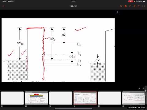
- Work function is the energy difference between the Fermi level and vacuum level, and different metals and semiconductors generally have different work functions.
- When materials are joined, charge redistributes until their Fermi levels align, creating built-in band bending even without an applied gate voltage.
- Interface defects, broken bonds, and oxide trap or fixed charges can add non-ideal fields and make oxide bands slope rather than remain perfectly flat.
13:30
Flatband Voltage Cancels Built-In Band Bending
- Flatband voltage, denoted VFB, is the gate voltage required to counteract built-in effects and flatten the semiconductor bands.
- Its sign depends on the direction of the initial bending, which is related to the gate-semiconductor work-function difference and other stack charges.
- MOSFET gate-voltage analysis uses flatband as a reference before considering further band bending and channel formation.
16:15
Positive Gate Bias Drives Depletion and Inversion
- Starting from flatband, positive gate bias on a p-type body repels holes from the surface and creates a depletion region.
- During depletion the material remains p-type because the Fermi level is still closer to the valence band than the conduction band.
- With greater positive bias, electrons accumulate at the surface; when the surface becomes effectively n-type, the device enters inversion, which can progress from weak to strong.
19:20
Threshold Voltage and the Intrinsic Fermi Level
- The intrinsic Fermi level lies approximately midway between the conduction and valence bands and provides a common reference for identifying p-type or n-type behavior.
- For a p-type body, threshold marks the point where surface inversion becomes comparable in strength to the body doping; additional gate bias strengthens the electron channel.
- The lecture expresses the strong-inversion threshold condition as surface potential ψs reaching 2ψB, where ψB is the bulk potential relative to the intrinsic level.
26:00
MOS Gate Stack as Series Oxide and Semiconductor Capacitors
- The gate stack contains oxide capacitance Cox in series with a voltage-dependent semiconductor capacitance associated with depletion.
- Series capacitors divide applied gate voltage according to their capacitances, so the semiconductor surface potential receives only part of the external voltage.
- The semiconductor voltage drives band bending and channel formation, while voltage across the oxide does not directly create the channel.
31:30
Oxide Scaling Tradeoffs and the High-k Solution
- Parallel-plate oxide capacitance follows C = κε₀A/t, so smaller gate area or greater oxide thickness reduces capacitance.
- A smaller oxide capacitance takes a larger share of the applied voltage in the series stack, leaving less voltage to control the semiconductor surface.
- Thicker oxide improves resistance to dielectric breakdown, but high-k material such as hafnium oxide can raise capacitance without requiring an equally thin physical barrier.
39:00
Poly-Silicon Gates, Metal Gates, and Work-Function Control
- Heavily doped n+ or p+ polysilicon can behave like a conductor while allowing its Fermi level, and therefore its work function, to be tuned through doping.
- A metal gate has a material-dependent work function that is less directly adjustable, making work-function matching and flatband-voltage control important.
- High-k metal-gate integration was a manufacturing challenge as well as a materials choice, because gate materials must adhere and remain compatible with the oxide stack.
48:20
Threshold Voltage Knobs: Flatband, Doping, and Oxide Capacitance
- Flatband voltage is a major threshold-voltage control, and fabrication can tune it through gate-metal type and composition.
- Body doping concentration NA changes the Fermi-level position and bulk potential ψB, thereby affecting the threshold condition.
- Oxide permittivity and Cox also influence threshold voltage, but the dielectric is selected as part of the process technology rather than adjusted dynamically after fabrication.
55:00
Gate and Drain Bias Shape the MOSFET Channel
- When VGS exceeds threshold, inversion charge creates a conducting channel between source and drain; greater VGS makes the channel stronger.
- With small VDS, the channel remains relatively uniform and the MOSFET behaves approximately like a voltage-controlled resistor.
- Increasing VDS weakens the channel near the drain; at pinch-off, the drain field sweeps carriers across the depleted region.
1:00:50
Output Characteristics: Linear Region, Pinch-Off, and Saturation
- The output characteristic plots drain current ID against drain-source voltage VDS for fixed gate voltages.
- At low VDS, ID rises approximately linearly because the channel is continuous; increasing VDS eventually narrows the channel near the drain.
- After pinch-off, the current approaches saturation, and a larger VGS produces a higher current curve.
1:03:40
Transfer Characteristics: Drain Current Versus Gate Voltage
- The transfer characteristic plots ID against VGS while holding a nonzero VDS across the transistor.
- Below threshold, the simplified circuit-level model treats current as negligible; above threshold, a channel forms and ID rises with gate voltage.
- At VDS = 0, a gate-created channel can exist but there is no source-to-drain current because there is no driving voltage.
1:08:30
Subthreshold Leakage and Billion-Transistor Power Costs
- Real MOSFETs leak current even when considered off, including subthreshold drain current and a small gate current through the dielectric.
- The lecture compares an illustrative 1 nA leakage per transistor with an on-current example of 100 μA, then notes that 10⁹ devices leaking 1 nA each would sum to 1 A.
- At VLSI scale, aggregate off-state leakage can become a major design concern, motivating closer study of subthreshold behavior and semilog current-voltage plots.
Summary, takeaways, and chapters were generated by AI from the video's transcript and may contain errors. The video belongs to its creator, NorDIC Lab.