Lecture 12: Combinational Logic Gates in CMOS - Part 2
 Watch on YouTube →
Overview
CMOS combinational logic is built by expressing Boolean functions in sum-of-products form, mapping products to series NMOS transistors and sums to parallel branches, then creating the complementary PMOS network and sizing both against an inverter. The lecture extends this method to performance: stacked transistors add resistance and parasitic capacitance, input history and body effect shift delays, and design choices such as limiting fan-in to about four, placing the slowest signal near the output, and restructuring logic manage trade-offs among speed, area, and power.
Key takeaways
- Convert a Boolean function to sum-of-products before mapping it to CMOS: series NMOS devices implement each product term, parallel NMOS branches implement the sum, and the PMOS network uses the complementary topology.
- For a reference inverter with NMOS width W and PMOS width 2W, an n-device series stack needs roughly n times the corresponding reference width per device to keep total path resistance near the inverter's resistance.
- Stacked-transistor body effect depends on internal-node voltage and input history, so a multi-input gate can have different switching thresholds and propagation delays for different input combinations.
- Deep series stacks hurt performance through both increased resistance and additional internal capacitance; fan-in around four is a practical target, with NAND pull-down and NOR pull-up paths becoming the respective bottlenecks.
- For a series stack, placing the latest-arriving input nearest the output lets earlier inputs precondition internal nodes before the critical signal arrives.
- Timing differences between logic stages can produce glitches, while wider devices used to improve drive increase short-circuit current; reducing unnecessary transitions and balancing area against speed are essential design choices.
Chapters
- NMOS transistors form pull-down paths to ground, while PMOS transistors form pull-up paths to VDD.
- Represent Boolean functions in sum-of-products form: product terms map to series devices and sum terms map to parallel branches.
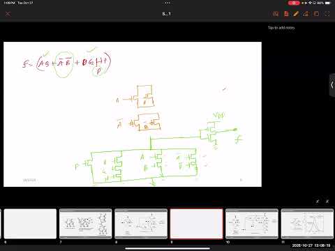
- The example function is AB + A'B' + DGH + P; redundant terms such as AB and ABC can be simplified using Boolean algebra.
- The NMOS network uses series devices for AB, A'B', and DGH, with those product branches and the single-device P branch connected in parallel.
- Assume complemented inputs such as A' and B' are available; this construction does not add input inverters.
- The PMOS network reverses each connection pattern: series NMOS blocks become parallel PMOS devices, and parallel NMOS branches become series PMOS blocks.
- An output inverter converts the pull-down network's complemented result into the desired output F.
- Use a reference inverter with NMOS width W and PMOS width 2W, a 1:2 strength-sizing assumption for the example.
- For a series branch of two NMOS devices, double each device's width so each has half the reference resistance and the branch totals approximately RN.
- For a three-device NMOS stack, triple each width; a single-device branch remains at the reference width.
- The PMOS-to-NMOS width ratio varies by technology, with the lecture citing historical 1:3, example 1:2, and modern values near 1:1.
- A PMOS pull-up path crossing four series devices has about 4RP if each device matches the inverter PMOS width.
- Make each device four times the inverter PMOS width to reduce its resistance to RP/4 and restore a total path resistance near RP.
- Because the reference PMOS is already 2W, the four-stack devices are each sized to 8W in the example.
- Check each conducting path so every transistor is accounted for; when path-based sizing demands conflict, the lecture recommends choosing the smaller requested size.
- During an inverter transition, NMOS and PMOS can conduct simultaneously, creating a temporary current path from VDD to ground.
- Drain current is approximately proportional to transistor width, so widening devices to balance pull-up and pull-down strength also increases short-circuit current.
- The design compromise is to accept greater transition current for balanced drive, while reducing unnecessary switching activity where possible.
- A two-input NAND has multiple input combinations, so its voltage-transfer characteristic can have different transition points for different input states.
- In a stacked NMOS path, an upper transistor's source may sit at an internal voltage rather than ground, reducing VGS and creating nonzero source-to-body bias.
- Body bias changes threshold voltage and therefore transistor strength; the bottom NMOS connected to ground avoids the same source-bias effect.
- Different internal-node voltages mean devices in a longer stack can experience different amounts of body effect.
- When one NAND input already holds its NMOS on, an internal node can discharge close to ground before another input transitions.
- If both series NMOS devices turn on together, stored charge on internal capacitances can leave the upper device with a nonzero source voltage.
- These different input histories produce different body biases, threshold voltages, and effective NMOS strengths, shifting the VTC transition point.
- For multi-input gates, evaluate the switching behavior separately for relevant truth-table input combinations rather than assuming one universal threshold.
- Every transistor junction and internal node contributes capacitance; model an on transistor as a low resistance and an off transistor as a high resistance.
- When a NAND output discharges, its load capacitance exchanges charge with internal-node capacitances before the full path reaches ground.
- Adding devices and branches introduces more RC nodes and charge-sharing paths, making charging and discharging more gradual than a single-resistor model suggests.
- A distributed resistor-capacitor network generally settles more slowly than one isolated RC load.
- Two transitions with the same final input values can have different delays because internal-node capacitors may or may not have discharged beforehand.
- If one input of a two-input NAND was already high, its NMOS had already discharged the intermediate node before the other input changed.
- If both inputs transition together, the output transition must also contend with intermediate-node charge and changing body bias.
- Characterize both fastest and slowest cases: slow paths affect setup timing, while overly fast paths can create hold-time problems.
- In a four-input NAND stack, a late-arriving input at the transistor nearest ground can block the discharge path while internal capacitors remain charged.
- If the late input controls the transistor nearest the output, earlier-arriving inputs can discharge internal nodes in advance.
- A useful timing rule for series stacks is to connect the slowest or critical input closest to the output and faster inputs closer to ground.
- The same ordering principle applies to series stacks on either the NMOS or PMOS side.
- Increasing NAND fan-in lengthens the series NMOS pull-down stack, requiring larger devices and adding internal capacitance.
- For a NAND gate, low-to-high charging can remain relatively steady because each PMOS pull-up branch has one device, while high-to-low discharge worsens with a deeper NMOS stack.
- A NOR gate reverses the bottleneck: parallel NMOS devices pull down, while series PMOS devices make the low-to-high transition increasingly difficult.
- Fan-in around four is presented as a practical sweet spot; deeper stacks are possible but can substantially degrade the slower transition.
- For a series PMOS stack in a NOR implementation, place the slowest-arriving input on the transistor closest to the output.
- Inputs on parallel branches are equivalent for this ordering rule because each branch connects directly to the output.
- For a six-input function, one deep gate can be replaced by smaller gates through logic reconstruction, trading additional area and connections for reduced stack depth.
- In a NAND chain, unequal gate delays can make downstream outputs switch temporarily even when their final logical values should remain unchanged; these unintended transitions are glitches.
- A glitch can propagate through later stages and become a full logic transition if the input timing does not settle in time.
- Input-output capacitance in a CMOS stage creates Miller coupling, which can cause an input voltage to overshoot slightly beyond VDD during a transition.
- Reducing unnecessary transitions and accounting for propagation delay helps limit glitch-related power and functional risks.
- In a multi-stage adder, carry arrives after the user-provided A and B inputs because it depends on the preceding adder; place the slower carry input near the output in a series stack.
- Progressive sizing can make the bottom NMOS in a four-device stack larger than the devices above it, compensating for its role in carrying the full discharge current.
- A six-input series gate can be reconstructed from smaller gates to reduce stack delay, but the resulting circuit may require more area and interconnect.
- CMOS design balances conflicting goals: compact area, adequate drive strength, low delay, and manageable switching power.
Transcript excerpt
0:00 that So, in the last class we discussed the key principle towards designing any combinational logic circuit. All right? We looked at a couple of examples. We talked about why NMOS transistors are necessary to uh design the pull down network, which brings down a node to zero. ground, right? We never use PMOSes to discharge nodes. We always use NMOSes to discharge and PMOSes to charge. Okay, we talked about the reasoning behind it. We talked about how to represent and and or logic with series and parallel connected transistors. And then we moved forward to start implementing random Boolean logic functions in NMOS network. And then whatever you do to the NMOS
0:47 network, you do the complementary connection in the PMOS network and you get a CMOS logic circuit. That's where we stopped, but actually we went ahead a little bit more. We also looked at sizing. We saw that when you have multiple transistors in series or parallel, it is necessary to size them up properly to balance the balance the charging and discharging branches. Okay? Don't worry, you don't have to remember everything. We are going to do one practice run today together. And hopefully everything will come back to us, all right? Let's do that. Let's use this page to do it from scratch. Let's start with a Boolean logic function. I would I would love to randomize it. Can anybody volunteer tell me a Boolean logic function? Please. >> AB or A not B not.
1:36 >> AB or A not B not. Okay. A Any Anything else to add to it? >> Or A times B times C. >> Or ABC. What else? Anything else? Please. No? So, by the way, just so you know, I'm going to be able to reduce it further to say, for
This is the start of the transcript. Save this video free for the whole transcript, searchable and time-coded.
Related notes
Summary, takeaways, and chapters were generated by AI from the video's transcript and may contain errors. The video belongs to its creator, NorDIC Lab.