Lecture 1: MOSFETs & FinFETS - A Quick Overview
 Watch on YouTube →
Overview
This lecture builds a MOSFET explanation from semiconductor doping: phosphorus and boron create mobile carriers, while a gate's electric field can dynamically form or remove a conductive channel between source and drain. It also reviews MOSFET structure and naming, enhancement versus depletion operation, and the Fermi-level and energy-band concepts that explain carrier generation and semiconductor conduction; FinFETs are not covered in the transcript.
Key takeaways
- Doping sets a silicon device's baseline carrier concentration: phosphorus donors add available electrons, while boron acceptors create vacancies represented as holes.
- In an N-channel enhancement MOSFET, a positive gate voltage across an insulating oxide repels holes and attracts electrons, forming a channel between N-plus source and drain regions.
- The MOSFET gate controls channel formation through an electric field and remains insulated from the source-to-drain current path.
- Thermal excitation generates electron-hole pairs, so N-type and P-type silicon both contain minority carriers as well as their respective majority carriers.
- At nonzero temperature, the Fermi-Dirac occupancy probability is one-half at the Fermi energy, and increasing temperature broadens the transition between likely-filled and likely-empty states.
- A semiconductor's smaller band gap than an insulator's allows thermal energy to create mobile electrons and holes, enabling limited conduction.
Chapters
- The lecture recaps MOSFET fundamentals for an upper-level undergraduate course, assuming prior exposure to semiconductor basics.
- VLSI systems build upward from devices to circuits, logic gates, modules such as adders, and complete products such as phones and drones.
- Device behavior is the foundation needed to understand the circuit-design concepts covered later in the course.
- Semiconductors are useful not for matching metals as conductors or plastics as insulators, but because their conductivity can be dynamically controlled.
- Doping sets a material's baseline carrier concentration at fabrication, while later electric-field control provides dynamic operation.
- A circuit component whose conductivity can be tuned offers functionality unavailable from a fixed-conductivity metal or insulator.
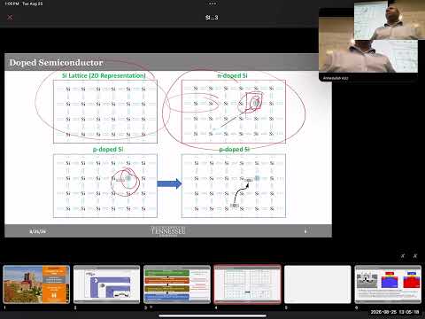
- Silicon has four valence electrons; pentavalent phosphorus has five, leaving an extra electron that is more available for conduction.
- Doping concentration, illustrated as 10^20 impurity atoms per cubic centimetre, controls the baseline number of available carriers.
- An N-type material has electrons as its majority carriers, but its doping level is fixed during fabrication rather than adjusted dynamically.
- Trivalent boron has one fewer valence electron than silicon and introduces an electron deficiency into the crystal.
- A hole is a useful representation of a missing electron: neighboring electrons move to fill vacancies, making the hole appear to move in the opposite direction.
- N-type and P-type materials both conduct through electron motion, although P-type conduction is commonly described using majority-carrier holes.
- Joining P-type and N-type silicon forms a P-N junction diode; combining three regions in an NPN or PNP arrangement forms a bipolar junction transistor.
- The MOSFET concept is motivated by controlling the middle region of a transistor structure so it can either block or enable source-to-drain conduction.
- A gate can switch the middle region's effective carrier type, creating an electronic switch controlled by voltage rather than by a mechanical contact.
- The gate must influence the semiconductor channel without carrying the source-to-drain current itself.
- An insulating oxide separates the gate conductor from the silicon, allowing the gate voltage to create an electric field across the oxide.
- The field changes the carrier distribution in the semiconductor underneath, providing a non-contact means of controlling conductivity.
- In the example N-channel MOSFET, heavily doped N-plus silicon forms the source and drain on either side of a P-type body.
- N-plus silicon is degenerately doped and highly conductive, making it suitable for connection to external circuitry.
- With no induced channel, the P-type region interrupts the electron path between the two N-plus terminals.
- N-type silicon has electrons as majority carriers and holes as minority carriers; P-type silicon has the reverse arrangement.
- Thermal energy can break a silicon bond and create an electron-hole pair, so both carrier types are present even in doped material.
- Thermally generated electrons and holes occur as pairs, unlike the majority carriers introduced by donor or acceptor doping.
- A positive gate voltage repels holes from the P-type silicon surface and attracts minority electrons toward the oxide interface.
- The initial removal of holes from the surface is depletion; accumulating electrons then creates a thin N-type channel.
- That channel connects the N-plus source and drain, allowing electrons to flow; removing the gate voltage eliminates the induced path.
- A practical MOSFET includes source, drain, body, gate, and an oxide layer beneath the gate, rather than only the simplified three-terminal drawing.
- Metal contacts and wiring connect the semiconductor terminals to external voltages and currents.
- Silicon oxide fills insulating regions and supports the device structure; these fabrication details are usually omitted from circuit symbols.
- An enhancement MOSFET is normally off and requires gate voltage to form its channel; a depletion MOSFET has a channel by default and requires voltage to turn it off.
- The lecture identifies enhancement devices as the type used in modern technologies and distinguishes N-channel from complementary P-channel MOSFETs.
- CMOS means complementary MOS, referring to the use of N-type and P-type MOSFETs whose responses to gate voltage complement one another.
- MOS describes the gate stack: metal, oxide insulator, and semiconductor beneath it.
- Modern gates can use metal, as in high-k metal-gate (HKMG) technology, rather than the heavily doped silicon gate material used in earlier structures.
- Field-effect describes how an electric field controls the channel, distinguishing this operating principle from the BJT's current-controlled junction behavior.
- At zero kelvin, the simplified Fermi-level model places filled electron energy states below the Fermi level and empty states above it.
- The Fermi level marks the boundary between occupied and unoccupied energy states in this idealized zero-temperature picture.
- At nonzero temperature, energy from the surroundings makes occupancy probabilistic rather than a perfectly sharp division.
- The Fermi-Dirac function gives the probability that an energy state is occupied by an electron, ranging from zero to one.
- At any nonzero temperature, the occupancy probability at the Fermi energy is one-half; increasing temperature broadens the transition around that energy.
- Thermal energy promotes electrons to higher energy states and leaves vacancies below, producing electron-hole pairs.
Transcript excerpt
0:19 All right. So, second I'm going to see which screen is getting recorded. Probably this one. Okay, that's fine. So today we'll start with a basic lecture. It's kind of like a recap of the key concepts covered on MOSFETs and pinpoints perhaps in other courses that you may have taken. Okay. So I'm assuming that you have taken other courses like 335 or something similar that teaches you the basics of MOSFETs or similar devices okay or at least
1:06 basics of semiconductors because this is supposed to be the one of the higher level courses for undergrads 400 level courses you cannot have anything higher than that in undergrad after that you have graduate courses right so but regardless uh I know it may be a while since you have taken those courses so I just want to make sure that we are all on the same page regarding some of the key concepts. So this is a highly condensed version of many of the concepts that you may have already seen. If not, it's great. You don't get too bored. But if you have seen them, just bear with us so we can all catch up together. Right now, more importantly, even before you start discussing anything, I highly recommend asking questions. You don't have to uh take it
1:53 in a way that hey maybe I'm the only one not getting it others are getting it. It's fine. Like I said if you start thinking about it this way hope at some point you'll probably lag behind the rest of the class. Chances are everybody else is not getting it either. So uh just go ahead and ask questions whenever they they appear in your mind. So we have seen this before. This is the level of hierarchy. uh we start with
This is the start of the transcript. Save this video free for the whole transcript, searchable and time-coded.
Related notes
Summary, takeaways, and chapters were generated by AI from the video's transcript and may contain errors. The video belongs to its creator, NorDIC Lab.