Lecture 11: Combinational Logic Gates in CMOS - Part 1
 Watch on YouTube →
Overview
CMOS combinational gates use an NMOS pull-down network to discharge the output and a complementary PMOS pull-up network to charge it; series connections represent AND conditions and parallel connections represent OR conditions. The lecture develops the network-construction method, explains why it initially produces an inverted function, and shows how to size transistor widths against a CMOS inverter reference while prioritizing worst-case paths.
Key takeaways
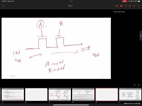
- In complementary CMOS logic, NMOS devices provide full-strength pull-down paths and PMOS devices provide pull-up paths; an NMOS pass device cannot charge an output to VDD because its VGS falls below threshold.
- Series-connected devices encode an all-inputs condition and parallel-connected devices encode an any-input condition, but the NMOS network's conducting condition discharges the output, so the resulting gate function is inverted.
- For a three-device series NMOS path, tripling each transistor's width reduces its on-resistance to roughly one-third, bringing the total path resistance back to the single-NMOS inverter reference.
- Parallel PMOS sizing depends on which branches conduct: three equal branches yield about RP/3 together, while a single active branch remains RP, so sizing for one case can impair another.
- When path balancing cannot cover every input combination, CMOS sizing prioritizes the worst-case conducting path instead of trying to make all possible paths identical.
- A final CMOS inverter restores the intended logic polarity and preserves rail-to-rail output swing, while Boolean reformulation is an alternative when it reduces total circuit cost.
Chapters
- A combinational circuit's output depends on the current combination of inputs, not their sequence or previous-cycle history.
- Digital inputs represent low and high, with VDD serving as logic 1 even when its voltage varies, for example 0.7 V, 0.9 V, or 5 V.
- The CMOS gate architecture shares inputs across NMOS and PMOS networks, which meet at the output.
- An NMOS with its gate at VDD can discharge an output node to ground while maintaining sufficient gate-to-source voltage.
- When an NMOS charges a node upward, its source voltage rises and VGS falls; conduction stops near VDD minus the threshold voltage.
- A PMOS has the complementary behavior: it charges a node effectively but loses strength as it tries to discharge one.
- These threshold effects motivate using NMOS devices in the pull-down network and PMOS devices in the pull-up network.
- Series-connected NMOS transistors conduct only when every controlling input is high, representing an AND condition such as A·B·C.
- Parallel-connected transistors conduct when any controlling input is high, representing an OR condition such as A + B.
- For direct network construction, map Boolean products to series connections and Boolean sums to parallel connections.
- For A + B + C·D + E + F·G, build parallel branches for A, B, C·D, E, and F·G.
- Implement each product, such as C·D or F·G, as a series transistor path, then connect the sum terms in parallel.
- The NMOS network connects between the output and ground; the corresponding PMOS network connects between VDD and the output.
- The order of devices in a series branch does not change its Boolean function, though placement can affect circuit performance.
- For the PMOS pull-up network, replace every NMOS series group with a parallel group, and every NMOS parallel group with a series group.
- For (A + B)·C + D·E, the NMOS uses parallel A/B followed in series by C, with a separate D/E series branch.
- The corresponding PMOS network places A and B in series, C in parallel with that pair, D and E in parallel, and the two larger subnetworks in series.
- PMOS devices turn on with low gate inputs, so the complementary topology provides pull-up behavior for the opposite input cases.
- An output value of 0 requires a conducting NMOS path to ground; an output value of 1 requires a conducting PMOS path to VDD.
- The complementary networks are designed so the required pull-up and pull-down conditions correspond to opposite input cases.
- Earlier NMOS-only resistor-load logic used a pull-up resistor; CMOS instead uses PMOS devices for active pull-up.
- The same series-and-parallel construction principle can describe older NMOS logic, even though that logic lacks the complementary PMOS network.
- The NMOS network activates to discharge the output, so its conducting condition makes the output low rather than passing a logic high.
- The constructed CMOS gate therefore produces the complement of the intended Boolean condition, such as an inverted AND output.
- One correction is to append a CMOS inverter; the other is to transform the Boolean expression and construct a network for the complemented function.
- Input complements such as A and A′ are assumed to be available from the logic input bus, while an output inverter adds real transistors that must be counted.
- Using NMOS devices for pull-up and PMOS devices for pull-down could avoid a final inverter, but would sacrifice full rail-to-rail output swing.
- An NMOS pull-up stops near VDD minus its threshold voltage, so the output cannot reach the full supply voltage.
- The lecture treats rail-to-rail operation from ground to VDD as a key CMOS advantage over logic families with reduced output swing.
- For a complex function such as an adder, implementing the given expression and adding an output inverter can be simpler than algebraically redesigning the network.
- A transistor's W/L ratio uses channel width W and gate length L; the lecture identifies W as the practical sizing control.
- Technology choices such as 65 nm and 45 nm define the standard gate length, while changing L may require specialized fabrication.
- A series chain of three NMOS devices implements an A·B·C discharge condition, and the resulting gate output is its complement.
- Treating an on transistor as a resistance connects device sizing directly to output charging and discharging speed.
- The design target is to make each pull-up or pull-down path comparable in drive strength to the corresponding branch of a CMOS inverter.
- Three equal NMOS resistances in series produce 3R; tripling each device's width reduces each on-resistance to about R/3.
- The three widened devices then have a combined resistance of approximately R, matching the inverter's single-NMOS path.
- Width increases drive current, while the gate length remains fixed by the fabrication technology.
- Three identical PMOS devices in parallel have an equivalent resistance of roughly RP/3 when all three branches conduct.
- Making each device three times narrower would yield about 3RP per branch and RP total when all three are active.
- That sizing becomes slow when only one branch conducts: the sole active path has resistance 3RP instead of the inverter reference RP.
- Because input combinations can activate one, two, or three branches, one sizing choice cannot balance every parallel-path case.
- The engineering rule is to size for the worst case rather than optimize a parallel network only for the case where every branch conducts.
- For a pull-up network, one active PMOS branch is the weakest charging case because it has fewer parallel current paths.
- If the worst case has one PMOS device in the path, retaining the inverter-reference width gives that path a comparable resistance.
- Other input combinations may then be faster or less balanced, an accepted tradeoff when perfect balance is impossible.
- For (A + B)·C + (D + E)·G, the NMOS network has an A/B parallel group in series with C, in parallel with a D/E parallel group in series with G.
- The PMOS network complements each connection: A and B become series, C becomes parallel with their group, and D and E become series with G in parallel.
- One end of the NMOS network connects to ground and the PMOS network connects to VDD; their remaining terminals meet at the output.
- The gate's output remains inverted relative to the written function unless the expression or output stage accounts for that inversion.
- Using an example inverter with NMOS width 1 and PMOS width 2, a two-device series NMOS path is sized to width 2 per transistor.
- A four-device series PMOS path based on the width-2 reference is sized to width 8 per transistor; a two-device path uses width 4 each.
- Different conducting paths can share devices and imply conflicting width targets, so the lecture recommends balancing selected worst cases rather than expecting perfect equality.
- The worked example closes with a promise of further practice on mixed series-parallel sizing.
Transcript excerpt
0:00 Let's get started. Our lecture today is a natural next step from CMOS inverter. And when I was teaching you CMOS inverter, I told you many times that this is basically the foundational circuit that all the other logic circuits are based on. So, in today's lecture, we'll talk about combinational logic gates. And let me first address the elephant in the room, the first word. What is combinational, right? Why is it combinational logic? So, combinational logic is a circuit that whose output depends on the combination of inputs, okay? Not the sequence of input, remember. Okay, did A come first and then B came and then C came? No, we don't care about the sequence or timing.
0:48 We care about the combination. When I'm evaluating my output, I'm looking at the available inputs and the combination of available inputs. And what do I mean by combination? Remember, we're talking about digital circuits here, okay? Digital circuit. And in digital circuit, you only recognize two levels, low and high. Zero and one. But one is not always one, you know? VDD is your one. VDD could be 0.9, VDD could be 0.7, it could be 1.5, it could be 5 V, it doesn't matter. VDD is logical one. So, I look at Imagine you have three inputs, input one, two, and say three. You see how many of these are zero and how many of these are one. And then you decide to provide an output accordingly based on how you design this circuit. So, the output of this logic circuit depends on the combination of input. And
1:36 there is no history involved. That is more important thing. History meaning we don't care what happened in the previous cycle to the output. Because there are some circuits that will consider the history
This is the start of the transcript. Save this video free for the whole transcript, searchable and time-coded.
Related notes
Summary, takeaways, and chapters were generated by AI from the video's transcript and may contain errors. The video belongs to its creator, NorDIC Lab.