Lecture 4 DRAM Part 2
 Watch on YouTube →
Overview
Shimeng Yu explains how DRAM’s 1T1C cells are sensed, refreshed, and laid out, connecting circuit behavior to retention failures and density limits. Key topics include sense-amplifier offset cancellation, the 64 ms refresh standard, leakage and Rowhammer, and the shift from trench capacitors and 8F² layouts toward stacked capacitors and denser 6F²/4F² designs.
Key takeaways
- DRAM refresh is a read-and-restore process: sensing restores the cell’s data, and a 64 ms refresh window requires the controller to revisit every row before retention loss becomes unacceptable.
- The cell’s sensing margin falls by approximately ΔQ/CS as leakage accumulates, making smaller storage capacitance and higher leakage especially dangerous for the weakest cells.
- GIDL can occur during retention when a low or negative wordline and a bitline near VDD/2 create a negative gate-to-drain bias that triggers band-to-band tunneling.
- Rowhammer turns repeated aggressor-row activations into a data-integrity and security risk; activation counting and controller limits are ways to mitigate the disturbance.
- Open-bitline arrays improve density by borrowing a reference from an adjacent subarray, but the separate noise environments can make sensing more noise-sensitive than in folded-bitline arrays.
- DRAM scaling must preserve cell capacitance despite shrinking dimensions, which drives taller capacitor structures, high-k dielectrics, and layouts that balance contact clearance against 6F² or 4F² density.
Chapters
0:00
DRAM Read, Write, and Restore Sequence
- Precharge equalizes the bitline and complementary bitline to approximately half of VDD before a row is activated.
- Turning on the wordline shares charge between the cell capacitor and bitline, producing a positive or negative ΔV for stored 1 or 0.
- The sense amplifier amplifies the differential signal and restores the cell’s charge; writes drive new data through the bitlines while the wordline remains open.
4:30
Sense-Amplifier Offset Cancellation
- Process variation, including threshold-voltage mismatch between NMOS devices, can make a cross-coupled sense amplifier favor 1 or 0.
- If the built-in offset exceeds the cell’s small ΔV, the sense amplifier can resolve the wrong value.
- An advanced design adds four transistors, including diode-connected devices, to compensate mismatch before normal sensing.
12:15
DRAM Retention and the 64 Millisecond Refresh Standard
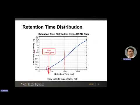
- Charge stored on a DRAM capacitor leaks over time, so cells must be refreshed to preserve data.
- JEDEC’s widely used refresh interval is 64 ms; the design must account for the weakest cells in the retention-time distribution.
- A refresh uses a read-and-restore operation: sensing recovers the stored value and writes it back without needing a separate data rewrite.
17:20
Scheduling Refresh Across DRAM Rows
- A refresh reads a whole row, and a row pointer must cycle through all rows within the 64 ms retention window.
- For 16K rows, the interval between row refreshes is about 64 ms ÷ 16K, or roughly 4 μs.
- During a row’s refresh, its bank or mat cannot serve an ordinary access; the controller queues requests and schedules work across other banks.
22:30
Cell Leakage and Its Effect on Sense Margin
- Stored charge can escape through reverse-biased P–N junction leakage, access-transistor subthreshold leakage, and capacitor leakage.
- The lecture’s sense-margin calculation subtracts the retention loss ΔQ/CS, where ΔQ is leakage current accumulated over the refresh interval and CS is cell capacitance.
- Because stored 1 places the junction under reverse bias while stored 0 may not, the 1 state generally has the more difficult retention condition.
28:10
GIDL: Gate-Induced Drain Leakage in Retention
- Gate-induced drain leakage (GIDL) occurs when a sufficiently negative gate-to-drain bias bends the silicon bands and enables band-to-band tunneling.
- The tunneling process generates electron–hole pairs; the resulting current drains charge from the storage node.
- During retention, the wordline may be held at zero or below while the bitline sits near VDD/2, creating the negative gate-to-drain condition that can produce GIDL.
33:30
Retention Bias and Disturb from Neighboring Cells
- Even when a DRAM cell is idle, its access transistor can leak because the drain-to-source voltage is nonzero.
- Activating an adjacent row can capacitively disturb a victim cell’s wordline; leakage can rise sharply as the victim’s gate voltage shifts.
- This dynamic disturbance makes retention depend not only on static cell leakage but also on activity in nearby rows.
37:00
Rowhammer: Repeated Activations Can Corrupt Neighbor Rows
- Rowhammer exploits repeated activation of an aggressor row, which can cause data flips in adjacent victim rows before the next refresh.
- Measurements on commercial DRAM show error rates rising substantially after roughly 10⁴–10⁵ activations in the described examples.
- Proposed physical explanations include charge movement through shared substrate regions and charge trapping near wordline sidewalls.
44:00
Rowhammer Controls and the Cost of Refresh
- A memory controller can count activations and limit or respond to rows that exceed an activation threshold.
- Refresh consumes time that could otherwise serve software requests; the lecture’s example estimates about 1% unavailability for a mat under its stated timing assumptions.
- Refresh also uses energy, and increasing DRAM capacity can raise both refresh overhead and power.
45:30
Trench and Stacked DRAM Capacitors
- Older trench-capacitor DRAM buried a deep capacitor in silicon; a cited 70 nm generation had an aspect ratio near 90:1.
- Modern mainstream designs use stacked capacitors above the access transistor, reversing the fabrication order used for trench capacitors.
- Stacked capacitors support denser layouts and make it easier to adopt high-k dielectric materials.
51:00
Array Limits and Folded-Bitline Architecture
- Longer bitlines increase bitline capacitance CBL and reduce the sensing signal; long wordlines also incur RC delay that scales approximately with length squared.
- A DRAM cell supplies only one data signal, so a folded-bitline array uses a separate cell on a neighboring row to provide the complementary reference.
- The folded arrangement staggers cell locations to keep the reference cell inactive during sensing, but wastes layout area and typically uses an 8F² cell footprint.
58:40
Open-Bitline Arrays Trade Area for Noise Sensitivity
- An open-bitline sense amplifier sits between two subarrays, sensing the selected subarray while the other supplies the complementary reference near VDD/2.
- This arrangement avoids the folded architecture’s staggered-cell conflict and enables a conceptual 4F² layout.
- Because the differential inputs come from separate subarrays, their noise patterns may be less correlated, weakening common-mode noise rejection.
1:00:10
Reading the Folded-Bitline Physical Layout
- The layout connects the wordline to the access-transistor gate, one transistor terminal to the storage capacitor, and the other through a contact to the bitline.
- In the illustrated folded layout, two adjacent rows share a bit contact, while empty regions account for the 8F² footprint.
- The capacitor may be implemented as either a trench or a stack; the top-view layout shows where contacts and cell structures must fit.
1:03:00
Why Modern DRAM Uses 6F² and Targets 4F²
- Mainstream layouts use 6F² rather than the idealized 4F² because contacts and the tall stacked capacitor need physical clearance.
- A common 6F² arrangement uses a transistor channel angled relative to the wordline and bitline, providing room for the capacitor to stand above the cell.
- A future vertical-channel transistor could reduce the footprint toward 4F² by moving the channel out of the substrate plane.
1:09:00
Alternative 6F² Cell Layout Variants
- The lecture compares Samsung’s angled-transistor layout with a Qimonda design that uses nonuniform pitch averaging 3F.
- A Micron proposal alternates transistor orientation so active regions can form a continuous pattern rather than isolated islands.
- Across these variants, the 2F-by-3F footprint preserves room for bitline and capacitor contacts.
1:11:30
Scaling Cell Capacitance with High-k Dielectrics
- DRAM sensing depends on maintaining storage capacitance CS while minimizing bitline capacitance CBL and controlling leakage.
- For a cylindrical capacitor, capacitance scales approximately with dielectric permittivity times perimeter times height, divided by dielectric thickness.
- As dimensions shrink, manufacturers compensate by increasing capacitor height and dielectric constant and reducing dielectric thickness; zirconium oxide-based high-k materials can have a dielectric constant near 40 versus about 4 for silicon dioxide.
- The lecture gives modern cell capacitance as roughly 5 fF, down from historical values around 20 fF.
Summary, takeaways, and chapters were generated by AI from the video's transcript and may contain errors. The video belongs to its creator, Shimeng Yu.