EECS 373 - Fall 2026 - Lecture 17: "DMA & PCBs"
 Watch on YouTube →
Overview
EECS 373 Lecture 17 explains how to move from breadboard prototypes to manufacturable PCBs, covering board materials, fabrication, layout constraints, CAD tools, and rapid alternatives such as laser ablation and conductive ink. It then explains DMA as a way to transfer peripheral data directly to memory while freeing the CPU, and gives practical guidance for using the course datasheet and reasoning about exam problems.
Key takeaways
- Solderless breadboards are convenient for early prototypes but can produce hidden shorts and unreliable connections, and signals above roughly 1 MHz should not be trusted on them.
- PCB fabrication constraints should shape component and layout choices early: hobby services commonly support about 6 to 8 mil traces and clearances, and vias require sufficient annular rings for drilling alignment.
- Readable silkscreen labels and assembly-aware panelization prevent avoidable debugging and manufacturing failures, especially for very small boards handled by pick-and-place equipment.
- DMA is most useful for repetitive bulk transfers, such as ADC-to-memory capture or memory-to-DAC playback, because it frees the CPU from copying each data item.
- Exam preparation should prioritize understanding datasheet functions, bus behavior, and waveform signatures over memorizing register syntax or protocol mode numbers.
Chapters
- Plan an approximately 11-minute presentation around 15 slides, allowing about one minute per slide rather than rushing through 20 to 30 slides.
- Start with a general concept, such as how motors work, then connect it to embedded systems and the final project.
- Solderless breadboards are quick to assemble but can be bulky, unreliable, prone to loose wires or hidden shorts, and unsuitable for trusted signals much above about 1 MHz.
- Devkits with common 0.1-inch headers make early hardware integration easy, but wired prototypes are often too bulky to evaluate wearable usability.
- PCBs provide smaller, more robust assemblies; flex PCBs use flexible substrates such as polyimide, while rigid-flex designs join rigid sections with flexible interconnects.
- Protoboards offer a practical middle ground for class projects, and carefully built versions may support signal integrity into the hundreds of megahertz.
- Copper traces form electrical connections, while vias connect copper layers; through-holes also mount components and connect board faces.
- Surface-mount components use PCB pads and generally occupy less space than older through-hole parts.
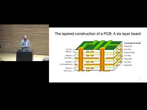
- Four-layer boards are common and affordable, while complex motherboards can use 16 or 20 layers.
- Multilayer boards are fabricated as layers that are laminated together, making precise alignment and via drilling important manufacturing challenges.
- A typical two-layer board starts with copper-clad FR-4, commonly about 1.6 mm thick, and uses Gerber files to define layer geometry.
- Manufacturing drills holes for vias and through-holes, applies photoresist, and etches away unwanted copper to leave traces.
- Solder mask protects exposed copper and limits solder bridging; silkscreen labels help with assembly and later debugging.
- Manufacturers may panelize small boards for production and assembly, so designs must fit pick-and-place equipment; boards that are too small can be impractical to assemble.
- Check three key fabrication limits early: minimum trace width, minimum clearance between signals, and via dimensions including the annular ring.
- Hobby board houses commonly support trace widths and clearances around 6 to 8 mil, with finer features often increasing cost.
- Use the chosen manufacturer's design rules in the CAD tool, and understand why a rule exists before deciding whether a design can safely depart from it.
- The core PCB workflow is to create a schematic, assign footprints, place components, route traces, and export manufacturing files.
- Choose footprints while designing the schematic, such as a 0603 resistor footprint or a through-hole alternative, and run design-rule checks before layout.
- For small boards, account for physical placement while choosing schematic connections; alternate microcontroller pins can avoid difficult routes.
- Gerber and drill files communicate copper geometry and hole locations to manufacturers, rather than passing along the editable design as the production definition.
- Cadence and Altium Designer are enterprise-grade options; the lecture characterizes Cadence as mature but difficult to use and Altium as feature-rich but increasingly bloated.
- Autodesk's Eagle, integrated with Fusion 360, provides layout and 3D visualization suitable for many student projects.
- EasyEDA is cloud-based and integrated with JLCPCB ordering, while that workflow may expose the full project to the manufacturer.
- For a single student PCB, several hobby-oriented tools can work; larger or multi-board projects may justify professional CAD tools.
- A lab fiber laser can ablate copper from raw PCB stock, enabling single- or double-sided prototypes in roughly 5 to 10 minutes after CAD preparation.
- Conductive-ink inkjet printing can create circuits on paper or transparent film, especially for sensors, though soldering is difficult and conductive epoxy may be needed.
- Conductive pens and vinyl cutters support interactive-book touch electrodes and large-area sensors; vinyl-cut traces generally need to be about 1 mm wide or wider.
- Conductive yarn, conductive 3D-printing filament, and room-temperature printed conductive plastic enable wearable circuits and body-mounted sensors.
- Direct memory access transfers data between a peripheral and memory without making the CPU execute every load and store.
- DMA is useful when data can be moved in bulk without per-sample decisions, such as ADC samples going into memory or a buffered waveform going from memory to a DAC.
- The CPU configures a DMA controller with source, destination, transfer count, and increment behavior; the controller can interrupt the CPU when the transfer completes.
- A DMA controller behaves like a fixed-function bus master rather than a processor that executes arbitrary code.
- The lecture distinguishes transfer arrangements called flow-through and fly-through, including cases where the DMA controller buffers data or configures a more capable peripheral.
- DMA channels provide constrained routes between peripherals and memory, so the number of simultaneous transfers is limited by available channel connections.
- The bus is presented as supporting concurrent channels rather than a single shared path; a routing table shows which peripherals can use which channels.
- A direct DMA path can move data between endpoints using fewer bus resources than routing it through the CPU.
- Prepare by mapping datasheet sections and software-library functions to likely design tasks, rather than memorizing every syntax detail.
- Know what helper functions do and how they fit together, while using the datasheet to check exact addresses and syntax during the exam.
- The instructor described roughly four or five design problems and advised preparing for familiar patterns, including a final C integration task.
- Focus on a workable architecture and relevant assumptions instead of perfect handling of every edge case.
- Identify communication protocols from waveform structure: SPI commonly uses chip select, while I²C shows clocked data and UART lacks a clock between transmitted bits.
- The exam emphasizes reasoning from waveforms rather than memorizing numeric SPI mode labels; a straightedge may help compare timing edges.
- Memory-mapped addresses and writing values to addresses are fair exam topics; reviewing load and store instructions is sensible, though assembly is not the main recent focus.
- The instructor named SPI as a preferred protocol for speed when chip-select wiring remains manageable.
Transcript excerpt
0:11 All right. Okay. We can get started. Today we'll talk about uh PCB design in general and then uh if there's time we'll talk about DMA. Realize you've already had a lab that used DMA but we can put a little bit more formalism behind it. Um and this will be the last formal lecture for me. Um so some we have student presentations start next week. So some general strategies these are going to be about 11 minutes. Um I usually think about presentations be about one minute per slide but then you also have like some intro slides maybe an exit slide. So maybe about 15 slides but I would not I always find it challenging when you have presentations that are just like jam-packed like 30 seconds or 15 seconds for a slide and you can't even grip what's on the slide and it's just going super fast. So I encourage you not to do
0:59 20 or 30 slides for 10 minutes. That would be amazing. Um maybe this is not the perfect uh structure but uh remember you are here to give an overview of this concept to people right? So what is how do motors work in general and then give them some context to their projects or projects that they would see in class. And so it's kind of like the general and then target down to what they would need to know for a particular um for their final project or how does it relate to embedded systems. Okay. So any questions on student presentations starting next week? Nope. Everybody's like, "Ah, next test this week. We don't have to come to
1:45 class." Okay, cool. That's fine. So I want to talk about PCB design. Um, so, uh, first we can think about the
This is the start of the transcript. Save this video free for the whole transcript, searchable and time-coded.
In this course
Related notes
Summary, takeaways, and chapters were generated by AI from the video's transcript and may contain errors. The video belongs to its creator, Interactive Sensing and Computing Lab.