EECS 373 - Fall 2026 - Lecture 14: “ADCs”
 Watch on YouTube →
Overview
EECS 373 Lecture 14 explains how sample-and-hold circuits prepare analog signals for conversion, then compares flash, single-slope, dual-slope, and successive-approximation-register (SAR) ADCs by speed, resolution, accuracy, power, and implementation cost. It concludes with practical configuration guidance for a microcontroller’s 12-bit SAR ADCs, including sampling time, channel multiplexing, oversampling, and conversion-time tradeoffs.
Key takeaways
- A sample-and-hold circuit lets an ADC measure a stable voltage by charging a capacitor while sampling and isolating it during conversion; weak or high-impedance sources may require longer sample time or a buffer.
- Flash ADCs achieve very high speed through parallel threshold comparisons, but resistor mismatch, comparator count, die area, and power make high-resolution versions costly.
- Single-slope ADCs trade conversion time for resolution by counting clock cycles until a ramp reaches the held input; faster clocks improve step size but increase power.
- Dual-slope integration improves measurement stability by measuring an input integration phase and a reference-driven return phase, canceling sensitivity to integrator resistance and capacitance.
- SAR ADCs use a DAC, comparator, and binary search to reach an n-bit result in a number of decisions proportional to n, making them a practical speed-resolution compromise for microcontrollers.
- Microcontroller ADC performance depends on the entire acquisition cycle: sample time, conversion time, channel multiplexing, bit depth, and any oversampling must fit the application’s sampling-rate requirements.
Chapters
- Project proposal meetings begin Friday or Sunday; teams should submit proposals the night before and bring presentation slides.
- The lecture follows prior analog-signal material and focuses on sample-and-hold circuits, ADC architectures, and the ADC on the course microcontroller.
- Reference materials include Chapter 20 of the course text and Analog Devices tutorials.
- An ADC needs time to measure an input, so a changing signal is captured on a capacitor and held steady during conversion.
- With the switch closed, the capacitor samples the input; opening the switch puts the circuit in hold mode.
- A buffer amplifier prevents the capacitor or ADC input from loading a weak source and distorting its voltage.
- The capacitor’s settling time depends on the effective resistance of the signal source: a weak source takes longer to charge it accurately.
- For sources such as a voltage divider or strain gauge, calibrate the reading and increase the programmable sample time if the measured value is low.
- A buffer can provide the sample capacitor with a stronger drive, while a lookup-table offset is a less reliable correction.
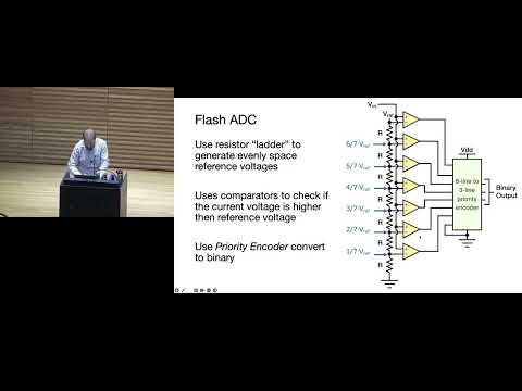
- A resistor ladder creates evenly spaced reference voltages, and parallel comparators report which thresholds the input exceeds.
- An encoder converts the resulting thermometer-like comparator pattern into a binary number.
- Because conversion depends mainly on comparator and logic propagation delay, a flash ADC can produce a result in roughly one clock cycle.
- Resistor mismatch shifts threshold spacing, making ADC steps nonuniform and reducing linearity.
- Resistors and many always-active comparators consume substantial silicon area and power; the hardware count also grows rapidly with bit depth.
- Flash ADCs are useful for very high-speed conversion, but cost and matching constraints commonly limit practical resolution compared with slower architectures.
- A single-slope ADC holds the input voltage, generates a rising ramp, and measures when the ramp crosses the input.
- A counter converts the crossing time into a digital value: a higher input takes longer to reach, yielding a larger count.
- A constant-current source charging a capacitor creates a linear ramp, unlike the exponential voltage rise of a basic RC charging circuit.
- Increasing the counter clock from a slow setting to a faster one produces more counts during the same ramp and therefore finer quantization.
- The maximum measurable voltage depends on the ramp’s range, while counter capacity must be large enough to hold the largest count.
- A faster counter increases digital switching and power consumption, so maximum clock speed is not always appropriate for low-power designs.
- A single-slope measurement depends on current and capacitance, both of which can vary with manufacturing differences and parasitic capacitance.
- Temperature changes can alter capacitor behavior and current-source performance, shifting the ramp rate and making measurements temperature-dependent.
- Factory calibration can correct fixed offsets; a temperature sensor and compensation table can help account for changes during operation.
- A dual-slope ADC first integrates the unknown input for a fixed interval, then applies a known reference current to drive the integrator back toward its starting point.
- Measuring the return time allows the capacitor and resistor terms to cancel, reducing sensitivity to component tolerances.
- Dual-slope conversion is slow but can provide high accuracy, strong noise and interference performance, and relatively low power; digital multimeters commonly use it.
- A successive-approximation-register ADC compares the held input against a trial voltage produced by an internal digital-to-analog converter.
- The SAR logic tests successive binary decisions, keeping or clearing each bit according to whether the trial voltage is below or above the input.
- Binary search converges in a number of steps tied to bit depth, rather than counting linearly through every possible value as a slope converter does.
- A four-bit SAR example makes four successive comparison decisions to approximate the held analog input.
- The result is the closest available quantized value, not necessarily the exact input voltage.
- A nominally higher-resolution SAR can convert faster when configured to stop before its least significant bits, trading precision for shorter conversion time.
- Resolution means the size of the smallest distinguishable step: dual-slope designs can achieve fine steps through longer measurement times, while flash designs are more constrained by ladder size and matching.
- Flash is the fastest architecture because its comparators operate in parallel; SAR offers a speed-resolution compromise, and slope integration is generally slower.
- Accuracy concerns repeatability and step consistency, not just bit count; dual-slope conversion reduces component-related error by canceling the integrator’s R and C factors.
- Flash ADCs typically consume the most power among the compared options because they use many comparators and a biased resistor ladder.
- Die-area cost is especially significant for flash designs, whose resistor ladders and comparator banks scale with resolution.
- Architecture rankings are approximate: implementation details and choices such as clock rate or conversion depth can change the tradeoffs.
- Sigma-delta ADCs use repeated one-bit measurements accumulated over time to represent the input.
- Pipeline ADCs divide conversion work across stages, allowing different portions of the conversion to proceed in parallel.
- These architectures are introduced as useful additional examples, rather than required exam material.
- The course microcontroller provides four 12-bit SAR ADCs, with multiple input channels per ADC selected through time-domain multiplexing.
- Configuration involves balancing sampling rate and resolution; selecting a faster rate or fewer conversion bits can shorten acquisition time.
- Hardware oversampling can combine repeated 12-bit readings to provide a 14-bit result, but requires extra conversions and is unsuitable at the highest sample rates.
- Calculate the maximum sampling frequency from both the programmable sample-and-hold interval and conversion time, which depends on the ADC clock and number of bit decisions.
Transcript excerpt
0:00 Let's see. Uh, you had James last week, so hopefully I don't know. You guys got through of analog sampling, I assume. Talk about analog circuits. Okay, great. So, that sets us up for this week. Um, so homework not due today. Today is not the 26th. That's scary. Next week. Next. All right. next Monday. And then homework 7's been released. It's not due for a couple weeks. Um, this week you guys need to sign up for project proposal meeting slots if you haven't already. Uh, they're going to start on Sunday or on Friday. Uh, we're not going to have class on Monday to make room for those uh, meetings. Um, and then your job
0:49 generally is to complete your project perfor proposal like the night before. So me and Matt will look through them in the morning, but also bring slides that kind of outline what you're going to uh be uh um presenting to us and what your project is. Um I mean, if you really had to, you could bring up your uh project proposal uh on the the monitor, but it's just easier if you have slides. Um and then we're going to give you feedback. So the project report askked for a lot of information. If you don't know the answer to every single thing because you haven't figured out what part it is yet, that's okay. but it's to try and prompt you to start thinking through things. If there are major issues with your report or maybe you just drastically change your project, well, there's a resubmission date where you can get back the points u and and kind of really the goal is for you to have a plan by the time you leave that meeting and finish
1:38 your project reports or proposals that
This is the start of the transcript. Save this video free for the whole transcript, searchable and time-coded.
Related notes
Summary, takeaways, and chapters were generated by AI from the video's transcript and may contain errors. The video belongs to its creator, Interactive Sensing and Computing Lab.