ECircuits-Lec8-2026
 Watch on YouTube →
Overview
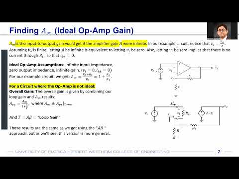
The lecture develops a feedback-based method for analyzing op-amp circuits with finite open-loop gain, non-infinite input resistance, and nonzero output resistance. It derives the closed-loop gain as A∞/(1 + 1/T), with loop gain T = Aβ, then shows how to find β by suppressing independent sources, modeling the op-amp, and multiplying voltage-division ratios; it also applies ideal-op-amp equivalent-resistance methods to homework examples.
Key takeaways
- A nonideal op-amp's closed-loop gain is A∞/(1 + 1/T), where A∞ is the ideal circuit gain and T = Aβ is the loop gain.
- Finite loop gain reduces the magnitude of closed-loop gain relative to the ideal result because the correction factor 1 + 1/T exceeds one.
- The feedback factor β is the returned differential input voltage divided by the output voltage, not simply the voltage at either input terminal relative to ground.
- To compute β, suppress independent sources, replace the op-amp with its resistance and controlled-source model, and multiply the voltage-divider ratios along the feedback path.
- An ideal op-amp can still be part of a circuit with finite input resistance: the worked inverting amplifier has Rin = R1 = 150 kΩ, despite the op-amp input resistance being infinite.
- For the worked ideal inverting amplifier, R2/R1 = 600 kΩ/150 kΩ gives gain −4, while its ideal circuit output resistance is zero.
Chapters
- The topic shifts from ideal-op-amp analysis to finding circuit gain when the op-amp itself is nonideal.
- Labs begin Monday, September 14; students are advised to complete each section's prelab before its session.
- Homework 2 contains three problems on nonideal op-amps and is due the following Monday.
- A nonideal op-amp has finite input resistance, so current can enter its inputs and ideal virtual-ground assumptions may no longer hold.
- Nonzero output resistance combines with the connected load to create voltage division and reduce the delivered output voltage.
- The op-amp model includes input resistance, output resistance, and a finite gain rather than ideal infinite input resistance, zero output resistance, and infinite gain.
- For a non-inverting amplifier with feedback resistors R1 and R2, the ideal gain is 1 + R2/R1.
- With the op-amp input drawing no current, the feedback network gives β = R1/(R1 + R2).
- The ideal closed-loop gain is 1/β, which recovers 1 + R2/R1 and connects resistor-divider analysis to feedback theory.
- The general feedback expression A/(1 + Aβ) can be written as A∞/(1 + 1/T), where T = Aβ and A∞ = 1/β.
- For an ideal op-amp, A is infinite, so T is infinite and the denominator correction 1/T vanishes.
- For a nonideal op-amp, finite T makes the denominator greater than one, so actual closed-loop gain is below the ideal value.
- To find T, use T = Aβ; the op-amp gain A is supplied by the problem or data sheet, leaving β as the circuit quantity to determine.
- Find A∞ by analyzing the circuit as an ideal op-amp, then calculate β as the fraction of output signal returned as differential input voltage.
- The method relies on familiar nodal analysis and resistor-divider calculations rather than solving every nonideal circuit from scratch.
- Suppress independent sources when finding β, then replace the op-amp with its input resistance, controlled source A·VD, and series output resistance RO.
- In the illustrated resistor network, calculate the return fraction through three divisions: RX/(RX + RO), RY/(RY + R2), and RA/(RA + R3).
- The intermediate equivalents are RX = R1 in parallel with (RA + R3), and RY = R4 in parallel with (R2 + RX).
- β represents the differential voltage across the op-amp input resistance as a fraction of the controlled output voltage.
- An op-amp can also be represented by a voltage-controlled current source with transconductance gm and a parallel output resistance.
- The controlled current gm·VD through its equivalent load resistance RL produces output voltage, giving voltage gain gm·RL.
- For the shown network, RL combines RO, R4, and the R2 + RX path; the feedback divisions still use RX/(RX + R2) and RA/(RA + R3).
- The assigned circuits ask for ideal gain A∞, overall circuit input and output resistance, and loop gain with op-amp gain 500, input resistance 100 kΩ, and output resistance 1 kΩ.
- For the worked inverting-amplifier example, R1 = 150 kΩ and R2 = 600 kΩ give A∞ = −R2/R1 = −4.
- To find nonideal loop gain, suppress the independent input source, include the 100 kΩ input resistance and 1 kΩ output resistance, calculate β, and multiply by A = 500.
- Circuit input resistance is found with a test source: for the worked inverting circuit, the virtual-ground input node makes Rin equal to the 150 kΩ input resistor.
- Circuit output resistance is distinct from the op-amp's own output resistance; with an ideal op-amp, RO = 0 creates a zero-ohm path, so the circuit output resistance is zero.
- The remaining homework circuits use the same feedback-divider and test-source methods; frequency response is deferred to a later class.
Transcript excerpt
0:00 Okay. So in the last lecture we were just looking into uh finding gain of non ideal operators. Uh till now what we have looked into uh is something that was mostly a recap of your earlier knowledge. Now probably today is the first class where you'll be learning something uh totally new which is how to find the gain if your opamp itself is non ideal. Right? So you'll have a op circuit. The circuit looks like a inverting amplifier but the opamp is non ideal. So how to calculate the gain in that case that's what we'll be uh looking into today. Uh before going into that uh please remember that your labs will start next week. So on Monday September 14th is the first day of the lab. So according to your lab section make sure that um you are ready with your prelab before your actual lab
0:49 session. Um I have also uploaded last year's one of the previous year's DA office hour one where they talk about how to solve these lab one problems. Okay. >> So, please look into that if you need a reference. But, uh, in general, please make sure that you are ready with the prelab before the actual lab session. Also, homework 2 has been uploaded. It will be due next Monday. And homework 2 is just three very simple questions based on non ideal opams. So, what we'll learn today and in Friday's class will help you to solve the homework two problems. All right. So we have looked into different kinds of opamp circuits in the previous few
1:38 lectures. Uh but in most cases or of course in all cases the opamp itself was ideal. That means opamp had an infinite input impedance. It has zero output impedance. It had infinite gain and so
This is the start of the transcript. Save this video free for the whole transcript, searchable and time-coded.
Related notes
Summary, takeaways, and chapters were generated by AI from the video's transcript and may contain errors. The video belongs to its creator, WISE Lab - UF ECE.