ECircuits-Lec3-2026
 Watch on YouTube →
Overview
The lecture develops voltage- and current-division methods for resistive networks, showing how to work backward from an output, combine equivalent resistances, and check gain expressions against the circuit’s signal path. It then applies estimation to amplifier homework examples, including a voltage-amplifier model with gain 100 and a transconductance model, before introducing ideal op-amp assumptions and real-device input and output resistance effects.
Key takeaways
- For a multi-stage resistor network, work backward from the output, reduce series and parallel combinations, and multiply the resulting voltage-division ratios.
- Current division is inverse with respect to the resistance in the branch being measured: the R4 branch receives a fraction R3/(R3+R4) of the current entering the R3‖R4 pair.
- A gain expression can be sanity-checked by counting division stages: series elements along the voltage signal path correspond to voltage-divider factors, while current branches that divert signal correspond to current-divider factors.
- In the A=100 amplifier example, a 10 kΩ source resistance and 30 kΩ input resistance reduce the amplifier input to 0.75Vs, so the overall gain is about 75 rather than 100.
- When RL≫RO, the output divider RL/(RL+RO) is nearly one; when Rs is comparable to Rin, input loading can materially reduce the signal before amplification.
- An ideal op amp assumes infinite input impedance, zero output impedance, zero common-mode gain, infinite open-loop gain, and infinite bandwidth, but real-device models must account for finite values.
Chapters
- Students outside the E department can borrow DAD boards for the semester and return them afterward.
- Teaching assistants plan to distribute boards one week before labs begin, with an announcement to follow.
- Voltage division gives a larger voltage drop across a larger series resistance; current division sends more current through the lower-resistance branch.
- For the introductory resistor-network problems, gain is treated as output divided by input, such as Vout/Vs.
- For time-varying AC signals, the stricter definition is the change in output divided by the change in input, expressed as dVout/dVin.
- For a linear resistive network, the voltage ratio and its small-signal derivative produce the same resistance-based gain.
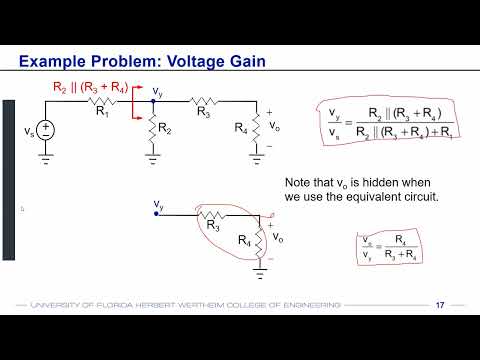
- Reduce R3 and R4 in series, then combine that equivalent resistance in parallel with R2.
- Use voltage division between R1 and the resulting equivalent resistance to find the intermediate node voltage relative to Vs.
- Apply a second divider across R3 and R4 to find the output across R4, then multiply the two voltage ratios.
- For faster calculator entry, divide numerator and denominator by the shared parallel-resistance term so it only needs to be evaluated once.
- In the illustrated circuit, the signal travels left to right through series-path resistors R1 and R3.
- The gain expression contains two voltage-division factors, matching the two series-path resistors that participate in division.
- If the output is defined across R3 instead of R4, the final divider changes from R4/(R3+R4) to R3/(R3+R4).
- Reduce the output-side network first: R3 and R4 are parallel, and their equivalent is in series with R2.
- Divide the source current between R1 and the compound branch, then divide the compound-branch current between R3 and R4.
- The current through R4 is its share of the second division, proportional to the resistance of the other branch, R3/(R3+R4).
- The overall current gain is the product of the two division ratios; its terms correspond to the two branches that divert current from the signal path.
- Homework problems 1 to 3 apply the same voltage- and current-division techniques to find voltage or current gain.
- For an amplifier model with A=100, a 10 kΩ source resistance and 30 kΩ input resistance produce an input ratio of 30/(30+10)=0.75.
- The amplifier’s internal output is therefore about 75Vs; a 100 Ω output resistance feeding a 10 kΩ load causes only a small additional drop.
- When a load resistance RL is much larger than output resistance RO, RL/(RL+RO) is approximately 1, making estimation more useful than reporting spurious decimal precision.
- A 10 kΩ source resistance substantially divides the input with a 30 kΩ amplifier input resistance, while a 10 Ω source resistance would make that division nearly disappear.
- In the second homework model, a 100 Ω source resistance feeding a 40 kΩ input resistance passes nearly all of Vs to the amplifier input.
- The model uses a dependent current source with gm=1 mA/V, equivalent to a transconductance of 1 mS, and a 200 kΩ parallel output resistance.
- The assumed current-arrow direction determines the sign of the output voltage; reversing the arrow reverses the sign.
- Amplifiers are treated as amplifying AC signals; a sine wave provides a simple single-frequency test input.
- An op amp has non-inverting and inverting inputs, with output modeled as A(V+−V−).
- The ideal model assumes infinite input impedance, zero output impedance, zero common-mode gain, infinite open-loop gain, and infinite bandwidth.
- Equal inputs make V+−V− equal zero, so an ideal differential amplifier has zero output and infinite common-mode rejection.
- Real op amps have finite input resistance, nonzero output resistance, finite open-loop gain and bandwidth, and nonzero common-mode gain.
- Finite input resistance Rin combines with source resistance Rs to form an input divider, so the op amp’s actual input voltage Vi may be lower than Vs.
- A nonzero output resistance Ro and load RL form another divider; the output approaches the internal source voltage when RL is much greater than Ro.
- In the dependent-source model, the amplified output is A·Vi, where Vi is the voltage developed at the op-amp input after source loading, not automatically the original source voltage.
Transcript excerpt
0:03 All right. Uh first off, there were questions regarding the dad boards. Uh that I know most of the E students already have access to the dad boards. Uh however, if you're outside of the E department, let's say a major from a different department, then uh we are going to lend you that boards for the semester and you'll have to give them back at the end of the semester just like uh any other courses that you have taken at E. um the TAS will be handing out those uh dad boards and that would happen one week before the lab start. So we'll make an announcement related to that. Okay. So in case you are looking for a dad board um I saw that there were seven responses in the group me chat that I had sent. Uh but I'm assuming that maybe there could be more students who need
0:50 the dad board for the semester. So I will be um I I'll mention that maybe around 15 students will need the dad boards. >> Okay. >> But do let me know in case you don't have one. >> All right. So we have started discussing some of the very basic constructs of electrical circuit design. Of course we looked at Ohms law, KVL, KCL and their different applications. uh something that is going to be important for your homework one is the theory of voltage division and current division and in the last lecture we had started looking into u these techniques which we'll be using uh to solve the problems in your homework one now for many of you
1:38 this could be just a repetition just a primer uh because you might already know these concepts but I would still like to go over them uh because there are
This is the start of the transcript. Save this video free for the whole transcript, searchable and time-coded.
Related notes
Summary, takeaways, and chapters were generated by AI from the video's transcript and may contain errors. The video belongs to its creator, WISE Lab - UF ECE.