ECircuits-Lec5-2026
 Watch on YouTube →
Overview
The lecture connects amplifier voltage-transfer curves to practical operating conditions: an amplifier needs a DC bias point in its high-slope region before small AC signals can receive gain. It develops voltage-gain and decibel calculations, explains how source and load impedances reduce an op amp’s nominal gain, and introduces MOSFET and BJT small-signal models.
Key takeaways
- Deactivate independent sources only when calculating equivalent resistance; retain the original sources when finding open-circuit voltage or short-circuit current.
- Amplifier gain is the local VTC slope, so a useful Q point must lie in the steep region rather than either flat region.
- For a 0 V to 5 V amplifier, a bias near 2.5 V can provide signal headroom in both directions before the output reaches its limits.
- An op amp’s circuit gain can be lower than its datasheet gain because source and load impedances form voltage dividers; the worked example reduces nominal gain from 100 to 72.
- A MOSFET common-source stage has negative gain because increasing gate voltage increases drain current, which increases the drop across R_D and lowers the output voltage.
- Use 20 log10 for voltage ratios and 10 log10 for power ratios; the minus-3-dB bandwidth point corresponds to half power.
Chapters
- To find equivalent resistance looking into a port, deactivate independent voltage sources by shorting them and independent current sources by opening them.
- A test source measures equivalent resistance as R_eq = V_test / I_test; in the illustrated circuit, R_eq is R1 in parallel with R2.
- Keep the original sources active when finding open-circuit voltage or short-circuit current, since they produce the voltage and current being calculated.
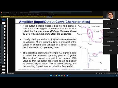
- A voltage-transfer characteristic (VTC) plots output voltage against input voltage; its slope, dV_out/dV_in, is the voltage gain.
- The example inverting VTC has a steep middle region where the magnitude of the slope exceeds 1, while its flatter regions provide little gain.
- A negative slope means an input sine wave is inverted at the output, producing a 180-degree phase shift.
- Biasing establishes a fixed operating point, or Q point, in the steep part of the VTC so small input changes produce substantial output changes.
- For an amplifier operating between 0 V and 5 V, a midpoint bias near 2.5 V provides room for the signal to vary in both directions.
- DC or large-signal analysis finds the operating point; AC or small-signal analysis then calculates gain around that point.
- Voltage gain in decibels is 20 log10(|V_out/V_in|), while power gain is 10 log10(P_out/P_in).
- A voltage gain of 10,000 corresponds to 80 dB; the factor of 20 follows from power being proportional to voltage squared.
- Using a logarithmic scale compresses large gain ratios into more manageable numbers.
- The local slope of the VTC at the Q point gives the amplifier’s small-signal voltage gain, A_v = dV_out/dV_in.
- Lowercase voltage and current symbols conventionally denote AC small signals, uppercase symbols denote DC or large-signal quantities, and mixed case can indicate both.
- The operating point is described by its input and output DC values, such as V_in,Q and V_out,Q.
- The basic small-signal model represents an amplifier with a dependent output voltage source A_v0V_in and a series output impedance Z_out.
- A more realistic model includes finite input impedance Z_in, finite open-loop gain, and limited frequency response.
- Adding parasitic resistances and capacitances improves agreement with laboratory measurements but makes circuit analysis more complex.
- The source impedance attenuates the input by Z_in/(Z_in + Z_source), and the output impedance attenuates the load voltage by Z_load/(Z_load + Z_out).
- The loaded gain is A_v0 multiplied by both voltage-divider factors; a datasheet gain assumes ideal source and load conditions.
- With R_source = 1 kΩ, R_in = 9 kΩ, R_out = 250 Ω, R_L = 1 kΩ, and A_v0 = 100, the realized gain is 100 × 0.9 × 0.8 = 72.
- A voltage ratio of 1 corresponds to 0 dB, 10 corresponds to 20 dB, and 0.1 corresponds to minus 20 dB.
- A 3 dB increase corresponds to a voltage ratio of √2 and a power ratio of 2; minus 3 dB corresponds to half the power.
- Amplifier bandwidth is conventionally measured at the frequency where gain falls 3 dB below its reference level, also called the half-power point.
- A MOSFET acts as a voltage-controlled current source: increasing its gate input voltage increases drain current.
- In the illustrated circuit, higher drain current creates a larger voltage drop across R_D, lowering the output voltage taken between R_D and the MOSFET.
- This inverse input-output relationship explains the negative gain and 180-degree phase inversion; at very low input, the MOSFET is cut off and the output approaches V_DD.
- The MOSFET model uses a dependent current source g_mV_GS, finite input impedance, and a parallel output resistance r_o.
- A BJT is modeled as a current-controlled current source, with output current approximately βI_B; its input current also needs an appropriate bias range.
- Both transistor types require a valid DC operating region before small AC fluctuations can produce amplified output changes.
Transcript excerpt
0:01 All right, so let's get started. First off, uh homework one is due tonight. So if you haven't yet completed, please do so by tonight, uh 11:59 p.m. Uh if you have any questions, I have office hours right after the class. So please feel free to meet me if you have any questions related to homework one or the course in general. Um All right. Now uh related to the and not
1:00 theorem I understand that there were a few questions after the class um during the last lecture as well and um I think I kind of misunderstood your question when you asked me that okay what happens with the not an equivalent circuit that uh when you are shortcircuiting the output how does the current flow right that was your question uh and I kind of misunderstood it in terms of the independent and dependent sources so what you are basically asking that how does the current flow if there is a no source inside the black box right that's what okay okay but related to that I think u I have uploaded a another PPD on treina and not an equivalence uh please go through that it's kind of like a recap of your 3le 1 uh however one thing that I would like to mention here that when you're trying to kill the independent sources that is
1:49 only to find the resistances so for example when you're looking even for the pe theorem when you're looking into the port the output port over Here you're trying to gauge what is the equivalent resistance looking from the right hand side. Okay. And in that case you see that there is R2 and then in parallel with R2 you have R1 because you need to short this independent voltage source.
This is the start of the transcript. Save this video free for the whole transcript, searchable and time-coded.
Related notes
Summary, takeaways, and chapters were generated by AI from the video's transcript and may contain errors. The video belongs to its creator, WISE Lab - UF ECE.