ECircuits-Lec30-2026
 Watch on YouTube →
Overview
The lecture develops a practical method for MOSFET small-signal gain analysis: establish the DC operating point, draw the AC equivalent circuit, determine the system's effective transconductance and output resistance, then include any input or output voltage division. Four configurations illustrate the method, including a common-source gain near -25, a degenerated gain near -4.17, a source follower near unity gain, and a common-gate amplifier; the lecture also derives finite-output-resistance effects and introduces body effect.
Key takeaways
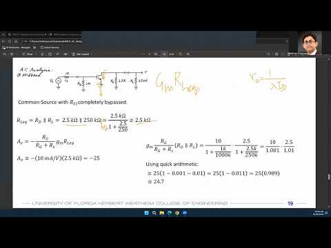
- For a common-source MOSFET with ID = 2 mA and VOV = 0.4 V, gm is 10 mS; with RD = 2.5 kΩ and a 250 kΩ load, the gain is approximately -25 when source degeneration is bypassed.
- A bypass capacitor across only part of the source resistance leaves the unbypassed portion in the AC path; 500 Ω of unbypassed resistance reduces the example gain to about -4.17.
- The general small-signal gain workflow is to find the circuit's effective transconductance and effective output load, multiply them, and then include any input or output voltage dividers.
- With finite MOSFET output resistance, unbypassed source degeneration raises the resistance looking into the drain to ro + (1 + gmro)RS.
- A source follower is a common-drain stage with gain near +1, while a common-gate stage is non-inverting; common-source gain is inverting.
- The recommended course sequence is Circuits I, Circuits II, then Analog IC I, which adds deeper models and topics such as body effect, noise, feedback, and layout.
Chapters
- The worked circuits use a DC drain current of 2 mA, threshold voltage VT = 0.6 V, and channel-length modulation parameter lambda = 0.
- With lambda = 0, the MOSFET output resistance ro = 1/(lambda ID) is treated as infinite.
- The goal for each example is to find the AC output-to-input voltage gain, building on bias analysis and homework examples.
- For VDD = 10 V and RD = 2.5 kΩ, ID = 2 mA gives a drain bias voltage VD = 5 V.
- With VSS = -5 V and RS = 2 kΩ, the source bias is VS = -1 V; the gate's DC voltage is 0 V because the coupling capacitor blocks DC and the gate resistor connects to ground.
- VGS = 1 V, so the overdrive is VGS - VT = 0.4 V; VDS = 6 V exceeds the overdrive, confirming saturation.
- At ID = 2 mA and overdrive 0.4 V, gm = 2ID/VOV = 10 mS, so 1/gm = 100 Ω; the corresponding process parameter is K = 25 mA/V².
- At sufficiently high AC frequency, the source bypass capacitor shorts the 2 kΩ degeneration resistor, leaving the transistor's gm as the effective transconductance.
- The output load is RD || RL, approximately 2.5 kΩ for RD = 2.5 kΩ and RL = 250 kΩ; the resulting common-source gain is about -25.
- A 1 MΩ gate resistor causes little input attenuation against a 1 kΩ source resistance, unlike a 1 kΩ gate resistor, which would halve the input.
- For AC analysis, VDD is an AC ground, coupling and bypass capacitors are shorts, and the MOSFET gate is an open circuit because of its insulating oxide.
- With source degeneration fully bypassed and ro infinite, the drain sees RD || RL; if lambda is nonzero, include ro in that parallel combination.
- The gain from the transistor gate to its output is -gm times the effective load resistance, with any input voltage division applied separately.
- The source resistor provides DC negative feedback: increased current raises the source voltage, reduces VGS, and stabilizes the operating point.
- In the second example, the source resistance is split into 500 Ω and 1.5 kΩ, with the bypass capacitor across only the 1.5 kΩ section.
- The unbypassed 500 Ω remains in the AC path, giving an effective transconductance gm,eff = gm/(1 + gmRS).
- Using the same transistor and output load as the prior example, the gain falls to approximately -4.17 instead of about -25.
- The circuit retains source resistance for DC bias stability while bypassing most of it to limit AC gain reduction.
- A source follower, or common-drain stage, takes input at the gate and output at the source; its gain approaches +1.
- The source-side resistance includes the external load and the MOSFET's small-signal resistance looking into the source, approximately 1/gm.
- A common-gate stage takes input at the source, grounds the gate for AC, and takes output at the drain; its gain magnitude follows the common-source form.
- Unlike the inverting common-source stage, common-gate gain is non-inverting because the input acts through VSG rather than VGS.
- For homework circuits, identify the system-level effective gm and effective output resistance, multiply them for gain, and account for input or output dividers.
- A gate bias divider with RG1 and RG2 appears as RG1 || RG2 to AC ground and can divide the signal with the source resistance.
- The common-source small-signal model uses a gmVGS controlled current source, optional ro, and RD connected to AC ground through VDD.
- Common-source gain is negative because increasing gate voltage raises drain current and the voltage drop across RD, thereby lowering the drain output voltage.
- With ro treated as infinite, source degeneration reduces effective transconductance to gm/(1 + gmRS).
- When ro is finite and RS is unbypassed, the resistance looking into the drain becomes ro + (1 + gmro)RS.
- The result follows from shorting independent input sources, applying a test voltage at the drain, and calculating the resulting test current.
- The factor gmro is the MOSFET intrinsic gain, so source resistance can boost drain output resistance by roughly intrinsic gain times RS.
- MOSFET bodies are commonly tied to the lowest potential for NMOS and the highest potential for PMOS to keep source-body and drain-body junctions reverse-biased.
- If the source moves away from the grounded body, a nonzero body-source voltage VBS produces body effect.
- A more detailed small-signal model adds a controlled current term gmB·VBS alongside gm·VGS and ro.
- Body effect is outside this course's analysis scope, but more advanced Analog IC courses include it and other MOSFET nonidealities.
- The recommended progression is Circuits I, then Circuits II, then graduate-level Analog IC I, so students establish fundamentals before using more complex models.
- Analog IC I revisits common-source, common-drain, and differential-amplifier gains before expanding into topics such as noise, feedback, and circuit layout.
- Analog IC I may use body-effect terms and other model details beyond the basic current-source and ro models used in the undergraduate circuits sequence.
- Students can take graduate courses as undergraduates, but should expect greater depth and complexity than in Circuits I or II.
- Circuits II and Analog IC I can overlap in MOSFET gain concepts, and the instructor says taking them simultaneously should be manageable for prepared students.
- Analog IC I may devote substantial time to foundational amplifier configurations because graduate students can arrive with varied undergraduate preparation.
- Digital design, flip-flops, and Verilog familiarity can help with digital-side courses, while students without that background may need extra effort.
- More complex transistor models change the equations but preserve the basic analysis approach of drawing an equivalent circuit and finding gain.
Transcript excerpt
0:00 So I just started the recording. So let's look into a few problems first uh and their solutions and then we'll be looking into a cheat sheet to solve any kind of MOSFET AC analytics problems. Um some of these examples I mean all of these are uploaded on your canvas. So um let's look at maybe three or four examples first. We'll also take a look at some of the examples or similar questions to your homework file and then uh we we'll we'll go into the cheat. So for all these exercises uh assume that your ID current that is the DC current flowing through the MOSFET is 2 milliampere. Lambda is equal to zero that means there is no channel length modulation. Um which also means one upon lambda ID which is the output resistance of the MOSFET that is infinite. V_T that is the threshold voltage of the
0:49 MOSFET is equal to 0.6 6 volts. Um so in the first scenario you or for all scenarios you basically try to find out what is your output AC voltage over input AC voltage or what is your overall AC gain. All right. So let's take a look at these problems one by one. So for the first problem you have your VDD set at 10 volts. You have a 2.5 kiloohm resistance. Um, of course, during the DC analysis, you have learned how to set these resistances that depending on the value of your IDQ depending on where you want to bias the transistor in homework 4, you are actually finding out what is the value of these resistances. Uh, here because you are assuming that you have already done the DC analysis,
1:37 um, we'll not be trying to find out what are these values of these resistances
This is the start of the transcript. Save this video free for the whole transcript, searchable and time-coded.
In this course
Related notes
Summary, takeaways, and chapters were generated by AI from the video's transcript and may contain errors. The video belongs to its creator, WISE Lab - UF ECE.