ECircuits-Lec29-2026
 Watch on YouTube →
Overview
The lecture develops a repeatable MOSFET AC-analysis method: find the effective transconductance with the output shorted, find output resistance with a test source, then include loading and input voltage division. It applies the method to common-source amplifiers, showing how source degeneration stabilizes DC bias while reducing gain, how a bypass capacitor restores AC gain, and why common-drain stages serve as buffers while common-gate stages suit current amplification.
Key takeaways
- For AC amplifier analysis, calculate effective gm with the output shorted, calculate output resistance using a test source with independent sources zeroed, then include load and input-divider effects.
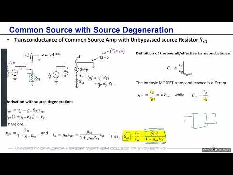
- Source degeneration changes effective gm to gm/(1 + gmRS); for gmRS much greater than 1, common-source gain approaches the process-insensitive resistor ratio −RD/RS.
- A bypass capacitor across the source resistor is open at DC and approximately a short at high frequency, combining bias stabilization with higher AC gain, though the restored gain depends on transistor gm.
- A common-drain source follower has gain gmRS/(1 + gmRS), near unity for large gmRS, and output resistance approximately RS || 1/gm, so it buffers high-resistance sources.
- A common-gate stage is noninverting and has input resistance near 1/gm, which makes it more suitable for current amplification than voltage amplification.
- The worked example’s 5 kΩ drain resistor and 20 kΩ load yield 4 kΩ output loading; with 2.9 kΩ source degeneration, the overall gain is about −1.14, rising to roughly −27 when the source resistor is bypassed.
Chapters
- Homework 4, 5, and 6 are due October 28, November 2, and November 9, respectively.
- Exam 2 is due November 9 and covers diode bias regions, MOSFET DC analysis, and AC gain in cascaded common-source and source-follower stages.
- Scott Morrison of Texas Instruments, who leads an analog and mixed-signal verification team, is scheduled for a mandatory-attendance guest lecture on October 28.
- Model voltage gain as effective transconductance multiplied by the equivalent output resistance, with a negative sign where the topology inverts.
- Find effective transconductance by removing the load, shorting the output, and calculating output current divided by input voltage.
- Find output resistance by zeroing independent sources and applying a test voltage or current at the output; combine it in parallel with the external load.
- A source resistor produces negative feedback: increased drain current raises source voltage, reduces VGS, and counteracts the current increase.
- The effective transconductance is gm/(1 + gmRS); when gmRS is much greater than 1, it approaches 1/RS.
- With transistor ro treated as infinite and drain resistance RD providing the load, the large-degeneration gain approaches −RD/RS, making gain less dependent on transistor process parameters.
- The example specifies ID = 1 mA, VD = 5 V, VS = 2.9 V, VG = 4 V, overdrive voltage 0.25 V, and transistor gm = 8 mS.
- For DC saturation checks, compare VDS with VGS − VT; the lecture focuses on the AC equivalent after establishing the bias point.
- At midband, coupling capacitors are treated as shorts and the DC supply is AC ground, so the 400 kΩ and 600 kΩ gate-bias resistors appear as 240 kΩ in parallel.
- With source degeneration RS = 2.9 kΩ, the effective gm is approximately 8 mS/(1 + 8 mS × 2.9 kΩ) = 0.33 mS.
- For RD = 5 kΩ and a 20 kΩ load, the output resistance is approximately 5 kΩ || 20 kΩ = 4 kΩ, giving a gate-to-output gain near −1.32.
- A 40 kΩ source resistance and 240 kΩ gate-bias equivalent produce an input divider of 240/(240 + 40), reducing the overall gain to about −1.14.
- A capacitor placed across the 2.9 kΩ source resistor is open at DC, preserving the negative feedback that stabilizes the bias point.
- At sufficiently high frequency, the capacitor shorts the source resistor for AC, so effective gm approaches the transistor’s 8 mS value.
- With the same 4 kΩ output load, the bypassed stage has a gain magnitude near 32 from gate to output and about 27 after the input divider, but this gain again depends on gm and thus process, voltage, and temperature.
- Input and output coupling capacitors create high-pass behavior, while transistor capacitances contribute high-frequency roll-off; the calculated midband gain lies between the cutoff regions.
- The source bypass capacitor adds another high-pass effect: gain is lower at low frequencies with RS in circuit and rises when the capacitor shorts RS.
- For common-source analysis, the small-signal MOSFET model uses a controlled current gmVGS; with ro infinite, the output load is RD and the gain is −gm_effRD.
- In a common-drain stage, the input is applied at the gate, the drain is the common terminal, and the output is taken from the source.
- When finding effective gm, remove and short the output load; the resulting transconductance is the transistor’s gm.
- The output resistance includes the external source resistor in parallel with the MOSFET’s resistance looking into its source, approximately 1/gm.
- Applying a test voltage at the source with the gate AC-grounded gives VGS = −Vx and a source current magnitude gmVx, so the MOSFET’s source-looking resistance is 1/gm.
- With source resistor RS, the output resistance is RS || 1/gm, and the exact unloaded voltage gain is gmRS/(1 + gmRS), approaching unity when gmRS is large.
- A source follower does not provide substantial voltage gain, but it can transform a high source resistance into a low output resistance; for example, gm = 200 mS gives 1/gm = 5 Ω.
- A common-gate stage applies the input at the source, grounds the gate for AC, and takes output from the drain; its VGS polarity is opposite that of a common-source stage.
- The output is noninverting: an increase in source input reduces drain current and the RD voltage drop, raising the drain voltage.
- Its source-side input resistance is approximately 1/gm, making it a poor voltage amplifier but a useful current amplifier; common-source stages suit voltage gain and common-drain stages act as buffers.
Transcript excerpt
0:04 All right, so let's get started. Um, first off, few announcements. Um, again, as you said, homework four to homework six has been posted. Please make sure that you know about the deadlines and submit them by um the required deadlines. Homework four will due on October 28, homework five on November 2 and homework six on November 9. Uh, the exam two has also been posted. uh please submit by November 9th which is two weeks from now. Um so you're getting two weeks for homework for for exam two and um let's quickly go through some of the problems. So of course the first problem is related to diodes and uh just make sure that you are uh considering the forward bias or the reverse bias region
0:51 of the diodes correctly for question number one and it should be very straightforward. Question number two is um 22 to4 is on MOSFET DC and AC analysis. So we are learning about BC analysis and AC analysis correctly. Uh today we'll take a look at a few more examples of AC analysis as well as how to solve some of the homework five problems and so on. But what you have for this particular problem is that you have a common source with source regeneration. So you already saw in um in some of the examples already that if you have a MOSFET and if your input is provided at the gate output is taken from the drain and if the source terminal is common between your input and output that's basically your common source configuration that's the configuration we have seen in most
1:38 detail till now. So you have a common source with this source regeneration resistance. uh of course there is a bypass capacitor sandle and we'll take a
This is the start of the transcript. Save this video free for the whole transcript, searchable and time-coded.
Related notes
Summary, takeaways, and chapters were generated by AI from the video's transcript and may contain errors. The video belongs to its creator, WISE Lab - UF ECE.