ECircuits-Lec26-2026
 Watch on YouTube →
Overview
The lecture develops MOSFET DC biasing and small-signal concepts, showing how to verify cutoff, triode, and saturation operation and how to calculate transconductance, output resistance, and gain. Worked NMOS examples use threshold voltages of 1.1 V and 0.7 V, device parameters such as K = 25 mA/V², and resistor-bias networks to find operating points and saturation limits; the next lecture will begin AC analysis.
Key takeaways
- For an NMOS, checking VGD < VT is an efficient saturation test because it follows from VDS > VGS - VT after the source voltage cancels.
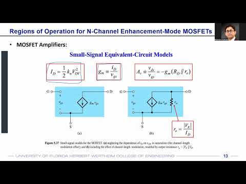
- In a common-source stage, the small-signal gain is -gm(RD || ro); it approaches -gmRD when the MOSFET output resistance is much larger than the drain resistor.
- The saturation boundary is VDS = VOV, so a fixed-current bias circuit can lose saturation as RD increases and the drain voltage falls.
- With K = 25 mA/V² and ID = 2 mA, the overdrive is 0.4 V; for the example with VS = -1.5 V, the minimum saturation drain voltage is -1.1 V.
- When source voltage and drain current are mutually dependent, numerical iteration can solve the bias point; the 6 V gate-drain-tied example with RS = 5 kΩ converges to about 0.93 mA.
- For a 10 V divider that must produce VG = 4 V and have a 40 kΩ parallel equivalent, resistor values are approximately RG1 = 100 kΩ and RG2 = 67 kΩ.
Chapters
- For an NMOS, cutoff occurs when VGS < VT; the device is on when VGS > VT.
- Triode operation occurs when VDS < VOV, while saturation occurs when VDS > VOV, where VOV = VGS - VT.
- In saturation, channel-length modulation gives ro approximately 1/(lambda ID), so output resistance depends on both lambda and the DC drain current.
- MOSFET transconductance is gm = dID/dVGS; in saturation, the lecture gives gm = K VOV, √(2KID), or 2ID/VOV.
- For a common-source stage, the source is shared by input and output and is grounded for AC analysis, even if it has a nonzero DC bias.
- Keep DC bias and AC behavior separate: a useful analog gain stage must first be biased in saturation.
- The output resistance is the Thevenin resistance seen from the drain, with RD connected to AC ground in parallel with the MOSFET's ro.
- The common-source voltage gain is approximately -gm(RD || ro), and reduces to -gmRD when ro is much larger than RD.
- The minus sign represents the common-source stage's inversion between gate input and drain output.
- The small-signal model represents drain current as a dependent source gm vgs, with ro placed between drain and source.
- For saturation with channel-length modulation, ro is approximately 1/(lambda ID); setting lambda to zero makes the idealized ro infinite.
- The transistor's intrinsic gain is gmro, analogous to an amplifier's open-loop gain; an external circuit can produce a lower overall gain.
- The NMOS example uses VDD = 7 V, VSS = -7 V, VT = 1.1 V, K = 25 mA/V², ID = 2 mA, and VD = 2 V.
- Ohm's law gives RD = (7 - 2 V)/2 mA = 2.5 kΩ.
- The saturation equation gives VOV = √(2ID/K) = 0.4 V and VGS = 1.5 V; with the gate at 0 V, the source is at -1.5 V and RS = 2.75 kΩ.
- Rearranging VDS > VGS - VT cancels VS and yields the convenient saturation test VGD < VT.
- In the 2 mA example, VG = 0 V and VD = 2 V, so VGD = -2 V, which is below VT = 1.1 V.
- The gate draws no DC current because the MOSFET gate oxide insulates it, so the drain and source currents have equal magnitude.
- With ID fixed at 2 mA, increasing RD increases its voltage drop and lowers VD while VS remains at -1.5 V.
- The saturation boundary is VDS = VOV = 0.4 V, giving a minimum drain voltage of VD = VS + VOV = -1.1 V.
- Using the stated 7 V supply and 2 mA current, the boundary calculation gives RD = [7 - (-1.1)]/2 mA = 4.05 kΩ; the lecture states approximately 4.4 kΩ, which does not match that arithmetic.
- For a gate-drain-connected NMOS, VGD = 0 V, so the saturation condition VGD < VT is automatically met for VT = 1.1 V.
- With K = 25 mA/V² and ID = 0.5 mA, VOV = 0.2 V and VGS = 1.3 V.
- If the tied gate and drain are at 6 V, then VS = 4.7 V and a source resistor to ground must be RS = 4.7 V/0.5 mA = 9.4 kΩ.
- With the gate-drain node at 6 V and RS = 5 kΩ, ID and VS are coupled: the MOSFET equation determines current from VGS, while the resistor sets VS from ID.
- The lecture demonstrates numerical iteration: guessing ID = 1.1 mA gives VOV ≈ 0.3 V and a resistor-implied current near 0.9 mA.
- Repeating the estimate converges to roughly 0.93 mA; each iteration recalculates VOV, VGS, VS, and the resistor current.
- For a divider spanning 10 V, setting VG = 4 V requires RG1:RG2 = 6:4; the additional condition RG1 || RG2 = 40 kΩ gives about 100 kΩ and 67 kΩ.
- The final bias exercise sets ID = 2 mA and VD = 6 V, then uses the saturation test, the MOSFET current equation, and Ohm's law to choose RD and RS.
- For that exercise, gm follows from K VOV and ro from 1/(lambda ID); the lecture closes by previewing MOSFET AC analysis and explaining why the divider's parallel resistance matters there.
Transcript excerpt
0:05 I like CMOS DC biasing as we had been discussing in the last lecture. That basically means that where do you want to place your transistor to make sure that it has some amount of gain. So, the first goal that all of us should have is to make sure that the transistor is placed in a region where you can expect gain out of it. And we have also looked into two different regions of operation. One of course the when the transistor is off, the equation for that is your VGS is lower than your Vth for the NMOS. Uh so, when the transistor is on, your VGS is going to be greater than the Vth for the NMOS. Now, of course for current to flow between drain to source or source to
0:52 drain, one of drain or source has to be at the higher potential. And for the NMOS, the drain will be at the higher potential, source will be grounded. For PMOS, you can think about the source being at the higher potential. And we have also looked into the equations for these different regions. We have proved how these equations are coming from uh the triode region basically says that your drain to source voltage VDS is lower than your overdrive voltage. If that happens, you're in triode. If your drain to source voltage is greater than your overdrive voltage, then you're in the active region or in the saturation region. And we have also seen these different regions in the um ID versus VDS characteristic as well. So, this is the output characteristic, ID on the x-axis, VDS on the ID on the y-axis and VDS on the x-axis.
1:41 And you have seen that in the triode region or the linear region, the current
This is the start of the transcript. Save this video free for the whole transcript, searchable and time-coded.
Related notes
Summary, takeaways, and chapters were generated by AI from the video's transcript and may contain errors. The video belongs to its creator, WISE Lab - UF ECE.