ECircuits-Lec25-2026
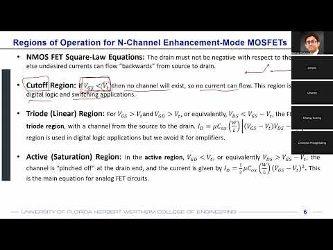 Watch on YouTube →
Overview
The lecture develops DC biasing and small-signal analysis for n-channel MOSFETs, connecting cutoff, triode, and saturation operation to digital switching and analog amplification. It derives the square-law drain-current model, channel-length modulation and output resistance, then shows how a common-source stage produces an inverting voltage-transfer characteristic and how transconductance sets voltage gain.
Key takeaways
- For an n-channel MOSFET in the ideal model, VGS below VT means cutoff, while an on-state is triode for VDS < VOV and saturation for VDS > VOV.
- Digital switching favors triode operation because low VDS makes the conducting MOSFET resemble a closed switch; analog amplification favors saturation because its output resistance is higher.
- The ideal saturation current ID = (K/2)VOV² is quadratic in overdrive, so doubling VOV produces four times the drain current.
- Channel-length modulation models the finite saturation slope with a factor of (1 + λVDS), yielding the approximate intrinsic output resistance ro = 1/(λID).
- For a common-source amplifier, biasing the Q point in the saturation region enables small-signal gain, with gm = KVOV and voltage gain approximately -gmRout.
- The same transconductance can be computed as KVOV, √(2KID), or 2ID/VOV, depending on which device and bias quantities are known.
Chapters
- Homework 4 covers DC biasing and large-signal operating regions, homework 5 covers AC gain, and homework 6 introduces an advanced MOSFET topic.
- Exam 2 is planned after homework 5 and covers diodes, some BJTs, and mostly MOSFETs; the deadline is discussed as falling around November 6 or 9.
- Solved examples for homework 4, 5, and 6 are available as practice, each using problems similar to but different from the assigned questions.
- The source arrow points outward for the illustrated n-channel MOSFET, indicating conventional current exits the source while electrons move from source to drain.
- An n-channel device requires positive VGS to attract electrons beneath the gate and establish a conductive channel.
- The output characteristic plots ID against VDS for multiple VGS values; increasing VGS strengthens the channel and raises the supported drain current.
- For the course's idealized model, VGS below threshold VT places the n-channel MOSFET in cutoff, with no formed channel and no drain current.
- Cutoff and an on-state correspond to an open and closed switch, respectively, making cutoff directly useful in digital logic.
- Real MOSFETs can still conduct subthreshold leakage; the lecture notes that many low-power research designs deliberately operate in this region.
- With VGS above VT, the device is in triode when VDS is below VOV, and in saturation when VDS exceeds VOV, where VOV = VGS - VT.
- Digital switch design favors triode operation because its low VDS approximates a closed switch with minimal voltage drop.
- Analog design favors saturation because ID changes relatively little with VDS, supporting current sources and high-gain amplifiers.
- The lecture links amplifier gain to gm times output resistance, so saturation's flatter ID-versus-VDS curve supports greater gain.
- The ideal saturation equation is ID = (K/2)VOV², with K = μCOX(W/L), combining process properties and device aspect ratio.
- Doubling VOV from 1 V to 2 V quadruples the ideal drain current, illustrated by an increase from 0.5 mA to 2 mA.
- This square-law relationship is a useful first-order model, but practical SPICE models are not exactly square-law devices.
- Increasing VDS moves the pinch-off point toward the source, shortening the effective channel from physical length L to L′.
- Channel-length modulation adds the factor (1 + λVDS) to the ideal saturation-current equation, creating a nonzero slope in the saturation region.
- The parameter λ has units of inverse volts; include the λ term when a problem specifies channel-length modulation, otherwise use the ideal square-law equation.
- The lecture compares this MOSFET effect with the Early effect in BJTs.
- Output conductance is go = ∂ID/∂VDS, the local slope of the output characteristic, and output resistance is ro = 1/go.
- Using the channel-length-modulation model gives go approximately equal to λID and ro approximately equal to 1/(λID).
- Although ro is a small-signal AC quantity, its value depends on the DC bias current ID.
- The MOSFET has intrinsic output resistance even without an external load; an external series resistance adds to it in the example discussed.
- A common-source stage uses a grounded source, gate input VGS, drain resistor RD connected to VDD, and drain voltage as the output.
- As VGS rises above VT, ID increases, the drop across RD grows, and VDS falls, so the output voltage moves in the opposite direction from the input.
- The device enters saturation just above threshold because VOV is small while VDS is initially near VDD; further input increase eventually pushes it into triode.
- The VTC has its steepest useful slope in saturation, while cutoff and triode provide little voltage gain.
- A nonzero DC gate bias sets the quiescent operating point near the middle of the VTC's saturation region, leaving room for an AC input signal.
- A small input variation around that Q point creates a larger output variation; the local VTC slope represents voltage gain.
- The lecture corrects a misplaced dotted line in a textbook-derived illustration, emphasizing that output levels should follow the actual VTC intersections.
- Small-signal transconductance is gm = ∂ID/∂VGS; differentiating ID = (K/2)VOV² gives gm = KVOV.
- Equivalent forms are gm = √(2KID) and gm = 2ID/VOV, allowing calculation from whichever of K, ID, or VOV is provided.
- The common-source voltage gain is approximately -gmRout; the negative sign indicates the 180-degree inversion as input rises and output falls.
- The lecture ends by setting up solved MOSFET examples for the next class.
Transcript excerpt
0:00 All right. So, let's get started. First round of announcements. So, of course, we have been discussing about MOSFETs. We have actually just started discussing on MOSFETs in the last few lectures. We have looked into the IV characteristic of the current and voltage characteristic for the MOSFET. And we have seen that the MOSFET is a voltage controlled current source. So, the output that we are looking at is a current, but that and on the other hand, the control that we have on the MOSFET is a voltage. So, the MOSFET is a voltage controlled current source, and that's where the IV characteristics comes from, the voltage versus current. And we have just started looking into DC analysis of the MOSFET. What does that mean? That means that you need to bias the MOSFET in a particular region to expect the correct performance out of it. What do we mean by the correct
0:48 performance? We'll see that later in more detail. Now, related to MOSFETs, I have uploaded the homeworks, and I have uploaded all the homeworks together related to MOSFET, so that you want if you wanted to get started on one of them early, you can do that. But, homework four will be due on October 28th. So, that's about 9 days from now. The week after, homework five will be due, and the week after, homework six will be due. Homework four is on DC analysis or biasing of the MOSFET. That basically means that where do you want to place your MOSFET in what operating condition and what operating regime, right? So, that's about the DC analysis or the large signal analysis of the MOSFET. On the other hand, homework five is about the AC analysis. That once you
1:37 have placed your MOSFET in the correct
This is the start of the transcript. Save this video free for the whole transcript, searchable and time-coded.
Related notes
Summary, takeaways, and chapters were generated by AI from the video's transcript and may contain errors. The video belongs to its creator, WISE Lab - UF ECE.