EECS 373 - Fall 2026 - Lecture 7: “Midterm 1 Review"
Overview
EECS 373's Midterm 1 review covers exam logistics and the embedded-systems concepts students need to apply: ARM Cortex-M4 assembly, memory-mapped I/O, GPIO configuration, and APB transactions. The review emphasizes using the supplied data sheet rather than memorizing details, tracing how loads and stores reach peripherals, and showing assumptions and work to earn partial credit on design problems.
Key takeaways
- Treat the course data sheet as the hardware-software contract: register access rules, reset values, address ranges, and pin mappings determine how software can use a peripheral.
- ARM addresses bytes, so a 32-bit word access usually spans four addresses; use the data sheet to locate implemented memory and peripheral registers rather than memorizing the full 4 GB map.
- For nested ARM calls, preserve the link register before making another branch-with-link call, and restore callee-preserved R4 through R11 plus the original stack pointer.
- An APB transfer completes only when PENABLE and PREADY are both high; a completer can hold PREADY low to insert wait cycles.
- Connecting a peripheral to an APB makes it accessible to software, but only the read and write capabilities specified by its programming interface need to be implemented.
- On design problems, stating a reasonable assumption, tracing the intended behavior, and showing intermediate work gives graders evidence for partial credit.
Chapters
- The exam is scheduled for Friday and uses three assigned rooms; students can find their room on the class assignment page.
- The exam is closed-book and closed-notes, but includes a fresh copy of the provided data sheet; a standard calculator is optional and phones must stay put away.
- State reasonable assumptions, show work, and attempt calculations or design steps to make partial credit possible.
- Homework 3 solutions are posted; plausible answers to the ambiguous final APB timing-diagram part receive credit.
- The course data sheet condenses information for the fictional Cortex-M4 used in lab, avoiding the scale of a full commercial manual.
- Treat a peripheral description as a contract between software and hardware: register behavior and access types define what each side must provide.
- Use pinout tables and alternate-function maps to identify which GPIO pins connect to peripheral signals.
- Study the data sheet before the exam; the design task is intended to be discoverable from its documentation.
- A reset value specifies a register's known state after power-on reset, for example a four-bit field documented as 0000.
- The PDM-to-PCM peripheral is tested through its inputs, outputs, and registers; students do not need to learn the audio formats in depth.
- The instructor identified and corrected register-address spacing errors during class, and flagged an invalid GPIO alternate-function entry for revision.
- Unreferenced protocol details in the data sheet, such as I²C-related material, are not required for the exam.
- Exam topics include ARM instruction encoding, load/store addressing, caller-callee rules, stack behavior, and memory-mapped I/O.
- Interrupts may appear as a conceptual question, but are not expected at the depth of a completed interrupt lab.
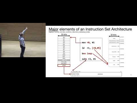
- The Cortex-M core uses 32-bit registers, including general-purpose registers and the program status register's ALU condition flags.
- Flags are used by conditional branches, but ordinary instructions do not update them unless an S suffix or comparison/test operation does so.
- ARM defines a 4 GB address space, but the manufacturer chooses which regions contain SRAM, flash, or peripherals and which remain unimplemented.
- Addresses identify individual bytes; a 32-bit word spans four consecutive byte addresses, so word-oriented access typically advances by four.
- SRAM is fast and volatile, while flash is nonvolatile and generally larger and slower; programs may be copied from flash to SRAM at startup.
- Peripheral registers also occupy addresses, but writes to them can trigger hardware behavior rather than simply store ordinary data.
- Use the supplied ARM appendix to look up instructions instead of memorizing the full instruction set; loads, stores, moves, adds, and branches are especially useful.
- An S suffix commonly requests updates to the program status register's ALU flags; flags can otherwise retain a value from an earlier operation.
- Conditional branches combine conditions such as the zero flag, with the appendix defining how conditions like equality map to flags.
- Assembler labels are resolved to actual addresses by the assembler and linker.
- A normal load reads from the address held in a base register; offset addressing adds an offset to form the effective address.
- Pre-indexing applies the offset before the memory access, and a writeback form updates the base register for iteration.
- Post-indexing accesses the original base address first, then applies the offset to the base register.
- For peripheral registers, a program can retain the peripheral's base address and use offsets, or use a full address directly.
- Registers R0 through R3 are scratch registers, commonly used for function arguments and return values; a caller cannot assume their values survive a call.
- A function must preserve R4 through R11 if it uses them, typically saving and restoring their original values on the stack.
- R12 is an intra-procedure scratch register, while R9 can be treated as a general-purpose register for this course.
- A subroutine must restore the stack pointer to its original position before returning.
- A branch-with-link call stores a return address in the link register; a function making another call must preserve its own return address first.
- Push and pop instructions that list multiple registers process them in register order, not necessarily in the written order.
- Separate push instructions execute in sequence, so their order must match the intended stack layout and later pops.
- Returning through the program counter can replace a separate move from the link register followed by a branch.
- The worked example calls a quad routine, which calls a square routine twice, illustrating how nested calls overwrite the link register.
- The quad routine pushes its return address before calling square, then restores that address before returning to its caller.
- Push advances the stack pointer to store data in the next stack location; pop retrieves it and adjusts the pointer.
- The exam generally rewards logically correct solutions rather than minimizing instructions unless the prompt specifies an efficiency constraint.
- A GPIO pin slice conceptually includes input, output, and control registers; control selects how the pin operates.
- A port register groups multiple pin values, with individual bits mapped to individual GPIO pins, so one word access can affect several pins.
- GPIO setup may require configuring both the pin's mode and its alternate function, as well as other peripheral-specific settings.
- Some microcontrollers provide bit-set or bit-clear registers to update selected pins and reduce unwanted output glitches.
- The core issues a store to an address; an APB requester checks whether the address belongs to a peripheral it serves.
- If the address is in its range, the requester generates bus address, data, clock, and control signals for the matching peripheral.
- The peripheral writes the value into a register, which may then drive a GPIO pin high or low.
- A complete explanation should trace the effect from the ARM store instruction through the register to the external pin.
- The review focuses on the Advanced Peripheral Bus connection between a requester or bridge and peripheral completers, not the more complex high-performance bus matrix.
- APB signals include PADDR, PWRITE, PSEL, PENABLE, PWDATA, PREADY, and PRDATA; each completer has its own response data and ready paths.
- The requester can present an address and data to the peripherals, while select and control signals determine which completer responds.
- The setup phase establishes stable transaction signals; the access phase uses PENABLE, and a completer can hold PREADY low to request wait cycles.
- PENABLE rises when the requester moves from setup toward access, after the transaction's address and control signals have been established.
- A transfer completes when PENABLE and PREADY are both high; PENABLE high with PREADY low represents a wait state.
- The completer determines whether it is ready, so the requester waits until PREADY is asserted before completing the transfer.
- Signals outside their valid phase, such as response data when a transfer is not enabled, may be treated as don't-care values.
- The example follows a word store to an address four bytes beyond a base address, with the write data labeled as the value being transferred.
- Address decoding selects the peripheral whose assigned range contains the target address; unused addresses may exist even within a reserved range.
- PSEL identifies the selected completer, while the requester establishes PADDR, PWRITE, and PWDATA before asserting PENABLE.
- For a simple register peripheral, PREADY may be asserted immediately; a slower peripheral can extend access with wait cycles.
- Begin by extracting the circuit's purpose and pin connections from its wiring diagram, then identify the device interface described in the problem.
- A timer or LCD sequencer is not automatically accessible to the core; it must be connected to the APB so software can reach it with loads and stores.
- Implement only the programming-interface capabilities specified by the data sheet, such as write-only access when no read capability is provided.
- Students may define reasonable registers or add notes about their design choices, but should explain unusual decisions to support partial credit.
- Read enough about a device such as a keypad to understand its operating sequence; the example requires driving scan lines to identify pressed keys.
- Use the design description and data sheet to plan what assembly or C code must do, including whether it needs to track state across operations.
- Write a brief strategy or intended behavior on the exam when uncertain; a correct plan can earn credit even if the implementation is incomplete.
- Extra scratch pages will be provided, and the supplied data sheet is the intended reference rather than a separate cheat sheet.
Transcript excerpt
0:00 All right, we can get get started. Let's see and push this there. Okay, so as we discussed the exam uh sheet was uh data sheet was released on Monday. I only saw one question I haven't had a chance to respond to, but this is your chance. If you have confusions about the data sheet, you can ask. Uh solutions for homework 3 were posted last night. There was a little uh confusion about the very last section uh of the design part about what to actually put on that APB di timing diagram because the question there's multiple ways to solve part three. So as long as you put down something that was plausible, you'll get
0:48 points. I don't you know I'm not going to penalize you for my error. Um, and I told I'll make sure the graders know that as well. And then uh exam will be on Friday. All this lecture is about going over the exams. Are there any questions to start with? Yes. >> Oh, yeah. Sorry. Well, yes, it's in DAO. In fact, we'll go over that in just a second, but thank you for pointing that out. Say that right now. And DAO. Nope, not Dowax. What other questions you got? All right, we'll get started. So, logistics, we'll do a course overview and if there's time, uh, we can walk through some of the design problems if
1:36 you would like. All right, so Oh man, you're right. These slides did not get open, get updated. Um, but that's not the exam location. We'll talk about that in a second. So closed books, closed notes, don't bring the reference sheet. So basically the packet that you have now, you'll get a fresh copy of it for the exam. Uh you can bring like a four function
This is the start of the transcript. Save this video free for the whole transcript, searchable and time-coded.
In this course
Related notes
Summary, takeaways, and chapters were generated by AI from the video's transcript and may contain errors. The video belongs to its creator, Interactive Sensing and Computing Lab.