EECS 373 - Fall 2026 - Lecture 4: “Memory Mapped IO / APB Bus
Overview
The lecture explains memory-mapped I/O in ARMv7-M systems: the core uses ordinary loads and stores to access peripheral registers, while hardware decodes addresses and routes transactions to the correct device. It develops the APB bus protocol, including shared address and data signals, per-peripheral selection, setup and access phases, and PREADY handshaking, then shows how address decoding and enabled registers can implement GPIO outputs.
Key takeaways
- Memory-mapped I/O lets an ARMv7-M core use ordinary loads and stores to access peripherals; the peripheral interprets register values as configuration or commands rather than general-purpose memory.
- APB reduces wiring by sharing address, write control, and write data across peripherals while assigning each completer its own PSEL line.
- An APB transaction has a setup phase and an access phase; PREADY completes the access or holds it open for wait cycles.
- Peripheral selection and register selection are separate operations: PSEL chooses the peripheral, while address decoding chooses a register inside it.
- External memory address ranges can be implemented by forwarding transactions through bus hardware, avoiding an impractical on-chip copy of the entire memory.
Chapters
- A microcontroller designed for 3.3 V may only tolerate a range such as 2.7 to 3.5 V, depending on its specifications.
- A voltage regulator provides a stable output as a battery drains, helping prevent changing timing or unexpected circuit behavior.
- Regulator selection depends on maximum input voltage, output voltage, current capacity, and whether the output is fixed or adjustable.
- The ARM memory map separates code, SRAM, peripherals, external memory, and external devices into address regions.
- Peripheral addresses identify hardware blocks rather than ordinary SRAM cells.
- A GPIO output register can store bits in D flip-flops, with those bits controlling the physical pin.
- Memory-mapped I/O assigns peripheral functions to addresses, so a store to a GPIO register can change an output pin.
- The same load-and-store model can access GPIO, timers, and other peripherals without processor-specific instructions for each device.
- The manufacturer’s datasheet specifies what each peripheral address and register does.
- A large external SRAM region cannot practically be represented by a matching bank of on-chip D flip-flops.
- An external bus unit can decode accesses in an address range and forward reads and writes to off-chip SRAM.
- The core sees memory-like addresses, while the bus hardware implements the transfer; the peripheral’s actual capacity depends on the manufacturer.
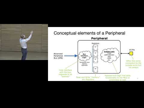
- A peripheral may contain several registers, such as GPIO configuration, output, and input registers.
- Loads and stores carry values to hardware, but peripheral logic interprets those values as commands or configuration.
- ARM defines the architecture, while the device datasheet documents manufacturer-specific peripheral functionality.
- A bus combines wires and supporting circuitry under a protocol for transferring data between locations.
- Parallel buses move several bits in one cycle, which is practical on-chip; off-chip parallel connections consume scarce physical pins.
- A shared bus avoids wiring every source directly to every destination and needs mechanisms to select the intended destination.
- A requester initiates a transaction; a completer performs the requested operation and does not start transactions independently.
- In the described architecture, an APB bridge carries requests from the core-side bus to peripherals.
- Address and read-or-write control identify the operation, while peripheral selection routes it to the intended device and register.
- The Advanced Peripheral Bus (APB) is a comparatively simple, low-power interface suited to peripherals that tolerate latency.
- The Advanced High-performance Bus (AHB) supports higher-throughput transfers and can accommodate multiple requesters, including DMA.
- The lecture focuses on APB; the bus choice depends on system goals such as speed, area, and power.
- The APB signals include PCLK, PADDR, PWRITE, PWDATA, PSEL, PENABLE, and PREADY; data is 32 bits in the lecture’s examples.
- PWRITE distinguishes writes from reads, while PADDR identifies the target register.
- The teaching examples treat PADDR as a 32-bit core address, but a real peripheral bus may use fewer address bits; roughly 4,800 mapped registers could require about 13 bits.
- During setup, the requester presents the address and operation and asserts the selected peripheral’s PSEL.
- PENABLE marks the access phase, when the peripheral can act on stable bus values.
- PREADY indicates completion during access; a low PREADY can extend the transaction with wait cycles.
- Address, write control, write data, clock, and enable are shared across APB peripherals.
- Each peripheral has its own PSEL, allowing the bridge to select one completer while the others ignore the transaction.
- Read-data paths are selected back at the bridge; the protocol describes the interface, while chip hardware can implement multiplexing internally.
- The class exercise maps a store of R0 to the address R1 + 4 onto transactions seen by two peripheral targets.
- Students identify the address, write direction, data, PSEL, PENABLE, and PREADY for each target.
- The exercise emphasizes that both peripherals can see shared address and data lines, but only the selected peripheral performs the write.
- For the example, R1 + 4 produces address 0x4, and the store sends the value in R0, shown as 0xC0FFEE.
- Both devices observe the shared address and write data, while PSEL is asserted only for the peripheral whose address range matches.
- The example uses a setup phase followed by access; a simple register write can complete in one access cycle when PREADY is high.
- PREADY matters to the requester during the access phase when PENABLE is asserted; a nonselected peripheral’s ready signal is ignored.
- A peripheral can hold PREADY low while it completes a slower task, extending the APB access.
- The lecture contrasts APB’s one-at-a-time peripheral transactions with AHB’s support for multiple channels or concurrent transactions.
- The LED example connects the least significant bit of a 32-bit GPIO output register to an external LED.
- Write data is captured by an enabled register only when the peripheral is selected, the access is active, the operation is a write, and the address matches.
- Because a simple register can capture data immediately, the example holds PREADY high rather than adding wait states.
- PSEL chooses a peripheral, not one of its internal registers, so address decoding must select the correct register.
- The example assigns register A to address 0x1000 and register B to 0x1004, with separate enable conditions.
- For homework and exams, write address masks in binary or hexadecimal instead of drawing cumbersome bubble logic, and label bus widths and bit positions.
Transcript excerpt
0:00 begin. Uh let's see. So today we're going to be talking about memory mapped IO, which is kind of like a new concept you probably haven't seen in 370 before. Uh some announcements. So homework's due today. Homework 3 was posted and it's due next week. And then office hours are today right after class from 3 to 4. If people need extra office hours, they can let me know. Um yes pro to normal lab schedules right all right so talk about component of the day how many people know what voltage regulators are then you'll actually learn something fantastic for the rest of you so last time we talked about batteries why can't you just connect up a battery straight to your device what's the problem.
0:55 You got your microcontroller. Oh, here we go. >> Drains drains over time. Which what is that? What's the implication for the electronics? Let's say it could tolerate that voltage range. What's the what's the challenge if it's changing its voltage over time? I saw I saw a hand. Somebody take a guess. You could be wrong. It's okay. Yes. >> Too low. >> Might get too low. Uh so yeah, it might get too low. So your uh electronics have a certain happy range which it was designed for. Usually your microcontrollers here are about 3.3. They might go up to like 3.5 maybe down to 2.7. Depends on the microcontroller. But internally, sometimes there's uh
1:43 analog components that are expecting a certain voltage and especially like uh oscillators or digital oscillators, they're all expecting a certain voltage so that the timing works out. And if all of a sudden you give it some weird voltage, this might have some unexpected behavior or at least that behavior might change over time. So sometimes your
This is the start of the transcript. Save this video free for the whole transcript, searchable and time-coded.
In this course
Related notes
Summary, takeaways, and chapters were generated by AI from the video's transcript and may contain errors. The video belongs to its creator, Interactive Sensing and Computing Lab.