EECS 373 - Fall 2026 - Lecture 5: “GPIO & MMIO”
Overview
The lecture connects ARM memory-mapped I/O (MMIO) to GPIO operation through the Advanced Peripheral Bus (APB): processor loads and stores become bus transactions that select peripheral registers and ultimately control physical pins. It explains APB setup, access, and wait states, then uses GPIO registers and pad circuitry to show how input, output, configuration, and alternate functions work, concluding with a register-level APB-to-GPIO design exercise.
Key takeaways
- MMIO lets the processor use ordinary loads and stores for peripherals: an address in the peripheral range causes the requester to generate an APB transaction instead of accessing SRAM.
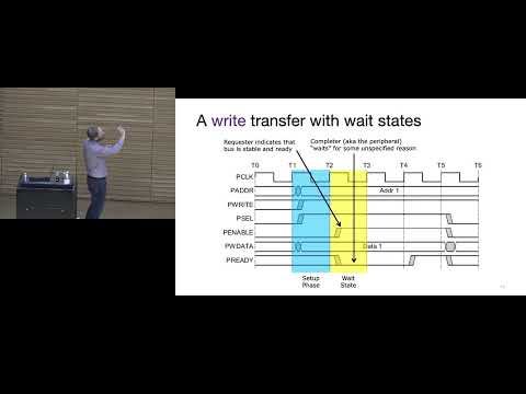
- An APB write should update a GPIO register only when the peripheral is selected, the address matches, and PWRITE and PENABLE are asserted; PREADY handles peripherals that need extra cycles.
- GPIO register bits connect software state to physical pins, so developers need the datasheet's addresses, bit fields, and pin configuration to predict the effect of a store.
- Internal pull-up and pull-down resistors provide defined input levels and can reduce PCB parts, while a 3.3 V GPIO input should not be assumed safe for 5 V signals.
- Alternate-function routing connects peripherals such as SPI directly to GPIO pads, and configurable drive strength and edge speed help balance load capability against ringing and overshoot.
Chapters
- A printed circuit board is a layered structure of etched metal traces that route signals between components.
- Pads provide soldering points, while holes or vias connect conductive layers.
- Standard component packages, such as 0603 resistors, make selecting PCB parts more manageable than a catalog of millions of components suggests.
- APB transfers have a setup phase, when the requester stabilizes signals, followed by an access phase when the peripheral can act.
- PADDR identifies a register, PWRITE distinguishes reads from writes, PSEL selects a peripheral, PENABLE marks access, and PWDATA carries write data.
- For reads, PRDATA carries peripheral data and PREADY indicates when the transfer can complete; data need not be valid before the peripheral is ready.
- Each peripheral has its own return path to the requester, so APB does not rely on multiple peripherals contending for one shared response bus.
- A read-only push-button example can sample a pin into a D flip-flop and return its value through PRDATA, with PREADY high when it can respond immediately.
- A writable register should latch PWDATA only when PWRITE, PSEL, PENABLE, and the matching address decode are all true.
- A register's output can remain available on its peripheral return path; the addressed register and read controls determine which data the requester uses.
- A peripheral inserts wait states by holding PREADY low during the access phase; the requester waits until PREADY rises.
- A temperature sensor may need several clock cycles to converge on a measurement before placing valid data on PRDATA.
- An SPI peripheral can accept a word over APB, then perform the serial transfer on its own clock and data lines.
- The die contains the processor, memory, and peripheral logic; bond wires connect die pads to metal package pins.
- A development kit's PCB traces route package pins to header pads that can be probed with an oscilloscope or logic analyzer.
- The terms chip and die are not interchangeable: chip is used broadly, while die refers to the unpackaged silicon.
- A basic GPIO port has input, output, and control registers plus pad logic for connecting internal data to external pins.
- Concatenating per-pin register bits creates a port-wide register, with each bit corresponding to a pin.
- To drive a pin, software stores a value to a GPIO register address; the requester turns the store into APB signals, and the peripheral updates the output register.
- The processor treats the operation as a memory write; software must know which register address and bit pattern control the external pin.
- The processor's memory map assigns address ranges to peripherals, and the requester selects the matching peripheral based on the target address.
- The requester controls the APB transaction's timing and signals; the peripheral can delay completion by holding PREADY low.
- Once PREADY is high, the peripheral must perform the read or write at the next rising clock edge.
- A pad is the physical pin interface, a port slice represents one pin's register and logic, and multiple slices combine into a port.
- The input path includes electrostatic-discharge protection, but a 3.3 V GPIO can still be damaged by an out-of-range 5 V input.
- The example device exposes 16 GPIO pins through registers whose useful data occupies the lower 16 bits, even when the register itself is 32 bits wide.
- Datasheet address patterns such as PN use the port number to identify the register block for a particular port.
- Dedicated set and reset register addresses let software change selected output bits without rewriting the entire port.
- Writing a one to a selected bit sets or clears that pin, while other bits remain unchanged.
- These are virtual register functions rather than separate physical storage registers, providing a lower-instruction-count alternative to read-modify-write.
- The example GPIO control scheme allocates five configuration bits per pin and uses multiple control registers to configure a port.
- Input modes can select plain input, pull-up, pull-down, or input inversion; configuration fields may also support other device-specific behaviors.
- A Schmitt trigger uses different rising and falling thresholds, rejecting small voltage fluctuations that could otherwise create false digital transitions.
- Noisy button waveforms illustrate why hysteresis helps, although it is not a substitute for every form of mechanical switch debouncing.
- Selectable internal resistors bias a GPIO input toward VDD or ground so an otherwise disconnected input has a defined logic level.
- Integrating pull resistors can reduce PCB component count and save board space, a useful advantage when device footprints are constrained.
- Programmable pull settings can also make a pin easier to reconfigure than a fixed external resistor.
- A push-pull output uses complementary transistor switches to drive a pin high or pull it low.
- An open-drain output disables the high-side transistor, allowing the pin to pull low or enter a high-impedance state.
- Open-drain signaling is useful on shared lines such as I²C because devices avoid simultaneously driving conflicting high and low levels.
- A pin's alternate-function setting can connect it to an on-chip peripheral such as SPI instead of ordinary GPIO control.
- Peripheral signals use a direct internal path to the pin rather than traveling through APB for each bit, avoiding unnecessary bus delay.
- A function-selection table in the datasheet identifies which bit pattern routes a peripheral signal to a particular pin.
- Pad-driver settings adjust output current strength and transition speed, with options described as weak or strong and soft, medium, or sharp.
- Fast edges and strong drive can cause overshoot or ringing when PCB traces and connected devices add capacitance or inductance.
- Reducing edge speed or drive strength can improve signal integrity; stronger drive may help with loads such as an LED, within the pin's limits.
- The exercise specifies APB signals and a simplified GPIO datasheet, then asks students to design a full port while wiring one representative pad.
- The design must support writing and reading the output register, reading the input register, and reading and writing the control register.
- Register widths follow the datasheet's 16 useful GPIO bits rather than requiring 32-bit storage for every register.
- Address decoding, PWRITE, PSEL, and PENABLE combine to qualify writes; a mux selects which register supplies read data.
- The walkthrough routes PWDATA to writable output and control registers, with address masks and APB control signals gating each register's write enable.
- A mux selects among the input, output, and control registers so only the addressed register drives the 16-bit PRDATA path.
- The pad's physical input feeds the input register, while the output and control registers drive the corresponding pad logic.
Transcript excerpt
0:21 All right, we can get started. Let's see. So, no real announcements. homework was posted yesterday, two days ago and is due on Monday. And then again, we have office hours after class on Mondays. And if you need you could contact me and we can find another time or there's also open open lab hours that you go to for help. Okay, so component of the day just PCBs in general just as a concept. They sound sometimes they sound overwhelming and scary, but really they are just layers of metal that have been etched into a sandwich and they're just wires. They're just routing from one place to another. The um I know OpenAI thinks they've solved it. They do all the PCBs for you. Uh I would be
1:08 surprised if it really works well, but we'll learn. It's another change to the industry. Uh PCBs have special features. We'll have a lecture on PCB design in general at the end of the semester, but there's things that are here. There are pads and that's what things get soldered onto. And then there's traces. Those are the kind of light green lines that just connect things. So again, it's just wires. And then they have some holes that allow you to go from one layer to another layer. And the other thing to kind of think about with PCBs is the entire industry has tried to standardize for maximum throughput and output, right? So like resistors and capacitors and transistors and all the IC types have very standard package sizes. So you can get a resistor in a very standard size is the number it doesn't matter but it's 0603 in any
1:57 variety you possibly want. So all you have to do is kind of once you kind of
This is the start of the transcript. Save this video free for the whole transcript, searchable and time-coded.
In this course
Related notes
Summary, takeaways, and chapters were generated by AI from the video's transcript and may contain errors. The video belongs to its creator, Interactive Sensing and Computing Lab.