Lecture 5: MOSFETS & FinFETs - Additional Concepts - Continued - v2
 Watch on YouTube →
Overview
FinFETs improve gate control over short channels by wrapping the gate around three sides, reducing drain-induced barrier lowering without the alignment problems of dual-gate designs. The lecture explains the tradeoffs this creates, including quantized transistor width and fin-pitch overhead, then connects continued scaling to velocity saturation, modern short-channel behavior, and the role of 3D integration.
Key takeaways
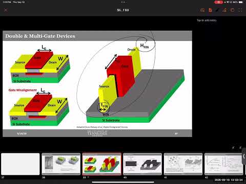
- A FinFET's gate wraps around the top and two sidewalls of its fin, giving three-sided channel control and avoiding the random alignment mismatch of separate dual gates.
- FinFET width is quantized as W = Nfin(2Hfin + Tfin), so designers adjust strength by adding whole fins rather than making the continuous width changes available in bulk MOSFETs.
- Fin pitch creates spacing overhead between fins, while neighboring gate structures add parasitic capacitance, so increasing fin count brings layout and circuit tradeoffs.
- Silicon's roughly 0.5 nm lattice constant means a hypothetical 3 nm channel spans only about six unit-cell lengths, highlighting why further planar scaling motivates vertical 3D integration.
- Modern short-channel MOSFETs can saturate through carrier velocity limits before the long-channel pinch-off condition VDS = VGS - Vth is reached.
- FinFETs reduce drain-induced barrier lowering, helping preserve on-current while improving subthreshold behavior and reducing off-state leakage.
Chapters
0:00
Why FinFETs Use Three-Sided Gate Control
- As MOSFET dimensions shrink, the drain increasingly interferes with gate control of the channel, motivating the move to FinFET structures.
- A FinFET gate controls the channel from three directions; the substrate prevents wrapping the gate around a fourth side.
- An early dual-gate approach used connected top and bottom gates, but it required precise alignment between two separate gate structures.
4:42
FinFET Gate Wrapping Avoids Dual-Gate Misalignment
- Random overlap and alignment errors between separate dual gates would vary across transistors and undermine predictable circuit behavior.
- A FinFET uses one gate structure that wraps over the fin and down both sidewalls, avoiding the separate-gate alignment problem.
- The fin has a process-defined height, Hfin, and thickness, Tfin, which are not freely adjustable by circuit designers.
10:00
Bulk MOSFET Width Is the Main Circuit-Design Strength Knob
- For a given process, mobility, oxide capacitance, channel length, threshold voltage, and supply voltage are largely fixed.
- Bulk MOSFET width can be varied to tune drive current and transistor strength without changing the source-to-drain barrier length.
- Reducing channel length is not a comparable free knob because short-channel effects and quantum tunneling grow rapidly as dimensions shrink.
14:08
Calculating FinFET Effective Channel Width
- Only the fin surfaces contacted by the gate contribute to the channel width; the gate overlaps the two sidewalls and the top of the semiconductor fin.
- The effective width of one fin is 2Hfin + Tfin: two sidewall contributions of Hfin plus the top contribution of Tfin.
- This perimeter-based width differs from the simple planar width used to describe a bulk MOSFET.
19:00
Fin Quantization Limits Fine Width Tuning
- Fabrication recipes fix fin dimensions, so designers generally cannot change Hfin or Tfin to adjust an individual transistor's width.
- Adding fins changes width in discrete steps: W = Nfin(2Hfin + Tfin), where Nfin is a whole number.
- This fin-width quantization is particularly restrictive for analog circuits, which often need finer strength adjustments than digital designs.
24:00
Multiple Fins Form One Device but Add Parasitics
- A multi-fin transistor uses a common source, common drain, and continuous gate connected across its fins.
- The fins are not independent transistors when their source, drain, and gate terminals are tied together; together they provide greater effective width.
- Adjacent conductive gate and fin structures can couple capacitively through the insulating material, adding parasitic capacitance.
29:00
Fin Pitch Creates Area Overhead
- Fin pitch is the repeat spacing between corresponding points on adjacent fins, and fabrication rules impose a minimum spacing.
- Unlike continuous bulk MOSFET width, FinFET layouts include gaps between width-contributing fins that consume area.
- As an illustration, a 1 nm gap relative to a 3 nm feature would represent a substantial fraction of the spacing budget.
33:30
Silicon Lattice Limits and the Shift Toward 3D ICs
- The silicon lattice constant is about 0.5 nm, so a hypothetical 3 nm channel spans only about six unit-cell lengths.
- Shrinking features toward only a few lattice cells makes continued two-dimensional scaling increasingly difficult.
- 3D integrated circuits address density limits by stacking structures vertically instead of relying only on smaller planar dimensions.
36:40
How TSMC and Fabless Chip Designers Enable 3D Integration
- TSMC is presented as a foundry that develops fabrication processes, while fabless firms such as AMD and Nvidia design chips made by foundries.
- Intel is contrasted as a company that both designs chips and operates fabrication facilities.
- Foundries demonstrate new process capabilities with research partners and customers before chip designers adopt them in commercial products.
45:50
Velocity Saturation Limits Modern MOSFET Current
- In semiconductors such as silicon, carrier velocity stops increasing proportionally with electric field once the critical field is reached.
- Scattering and interactions with the crystal limit electron motion, so higher applied field beyond the saturation point does not produce a proportional speed increase.
- Because carrier velocity contributes to drain current, velocity saturation limits current even when more voltage is applied.
50:30
Pinch-Off Versus Velocity Saturation
- In the long-channel model, pinch-off occurs when VDS reaches approximately VGS - Vth, limiting further drain-current increase.
- Modern short-channel transistors can saturate before that pinch-off condition because carriers reach saturation velocity first.
- The lecture compares the two limits to traffic: pinch-off narrows the road, while velocity saturation slows the cars even when the road remains open.
59:40
Constant-Voltage Scaling Raises the Electric Field
- Earlier constant-field scaling reduced supply voltage along with device dimensions, keeping electric field approximately steady.
- Threshold voltage cannot keep falling indefinitely because of leakage and the subthreshold-slope limit, so supply voltage also becomes difficult to reduce.
- Reducing channel length while maintaining voltage increases electric field and pushes modern MOSFETs into velocity-saturation behavior.
1:05:00
ID-VDS Curves Distinguish Long- and Short-Channel MOSFETs
- A long-channel MOSFET is expected to saturate near VDS = VGS - Vth; saturation at a lower VDS is a short-channel signature.
- In the long-channel saturation equation, drain current depends roughly quadratically on gate overdrive.
- With velocity saturation in short-channel devices, current depends more weakly and approximately linearly on VGS, producing more uniform current steps as VGS increases.
1:12:00
FinFETs Reduce DIBL and Off-State Leakage
- Drain-induced barrier lowering makes a transistor easier to turn on at higher VDS and can reduce effective threshold voltage as channel length shrinks.
- The Intel comparison shown in the lecture indicates that FinFETs reduce DIBL relative to planar MOSFETs while maintaining on-current.
- Reduced DIBL improves subthreshold behavior and lowers off-state leakage, explaining the benefit of three-sided gate control.
Summary, takeaways, and chapters were generated by AI from the video's transcript and may contain errors. The video belongs to its creator, NorDIC Lab.