Lecture 5: MOSFETS & FinFETs - Additional Concepts - Continued
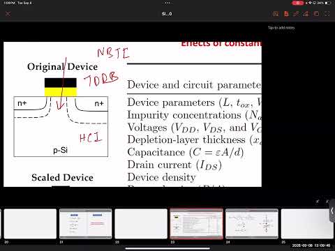 Watch on YouTube →
Overview
The lecture connects the end of conventional MOSFET voltage scaling to a core tradeoff: lowering threshold voltage boosts on-current but exponentially increases off-state leakage, while the roughly 60 mV per decade Boltzmann limit at 300 K constrains further improvements in subthreshold switching. It explains the resulting power, heat, and reliability pressures, then reviews approaches including strained silicon, high-k metal gates, and FinFETs, with gate-all-around transistors presented as a further way to strengthen gate control.
Key takeaways
- Reducing threshold voltage increases MOSFET on-current but also raises subthreshold off-current exponentially, making leakage from the many inactive transistors a major power cost.
- At 300 K, a conventional MOSFET with ideality factor M equal to 1 has a minimum subthreshold swing of about 60 mV per decade, the Boltzmann limit.
- Once threshold voltage stops scaling, lowering supply voltage reduces overdrive and on-current, while shared VDD rails prevent independently setting VDS to zero for off transistors.
- Strained silicon, high-k metal gates, and FinFET geometry address different constraints: carrier mobility, gate capacitance, and electrostatic control, respectively.
- Research devices can demonstrate sub-Boltzmann switching, including a cited 10 mV per decade result, but commercial adoption depends on scalable, affordable manufacturing processes.
- FinFETs improve channel control by wrapping the gate around three sides of a raised channel; gate-all-around devices extend that approach by surrounding the channel.
Chapters
0:00
Body Effect, Channel-Length Modulation, and Scaling Recap
- A MOSFET has gate, drain, source, and body terminals; body-to-source bias changes threshold voltage, including unintentionally in series-connected transistors.
- Channel-length modulation makes saturation current rise with drain-to-source voltage, producing finite output resistance represented by the parameter lambda.
- Constant-field scaling reduced dimensions and supply voltage together, but voltage scaling began to stall around the 65 nm generation.
3:15
Why Product Priorities Shape Voltage and Device Scaling
- Portable devices such as phones and smartwatches prioritize battery life, size, and heat alongside speed.
- High-performance computers and aircraft electronics can prioritize speed and tolerate greater power and cooling demands.
- Reducing transistor dimensions while holding voltage fixed raises electric fields across both the gate oxide and source-to-drain channel.
6:30
Electric-Field Stress, Soft Breakdown, and Chip Power
- Higher electric fields create reliability risks; gradual degradation is described as soft breakdown, in contrast to catastrophic failure.
- The lecture names TDDB, or time-dependent dielectric breakdown, NBTI, or negative-bias temperature instability, and HCI, or hot-carrier injection, as device degradation mechanisms.
- Maintaining supply voltage while increasing operating frequency raises power and heat; lowering supply voltage had previously helped reduce chip energy demand.
- Battery-powered devices cannot simply compensate for greater chip power with larger batteries without sacrificing portability.
13:00
Why Threshold Voltage Stopped Scaling
- Threshold voltage stopped scaling, which in turn constrained supply-voltage reductions.
- In saturation, transistor current depends on overdrive, VGS minus threshold voltage; reducing VGS while holding threshold voltage fixed reduces on-current and speed.
- Lowering threshold voltage could preserve overdrive at lower supply voltage, but it substantially increases off-state leakage.
16:50
MOSFET Subthreshold Current and the M Parameter
- The gate stack can be modeled as oxide and semiconductor capacitances in series, which divide the applied gate voltage.
- The lecture introduces the M parameter from this capacitive voltage division and shows it in the subthreshold-current equation.
- Below threshold, drain current depends exponentially on gate voltage and threshold voltage, making the M factor in the exponent especially consequential.
20:35
On-Current, Off-Current, and the Meaning of VDS
- The on-state is evaluated with VGS and VDS at VDD; the off-state has VGS at zero while VDS remains at VDD for the plotted ID-versus-VGS curve.
- Setting VDS to zero removes the source-to-drain energy difference and makes current approximately zero in the idealized explanation.
- With nonzero VDS and zero gate bias, the energy barrier remains, so off-current is small rather than exactly zero; tunneling and other secondary effects can still contribute.
27:30
The Threshold-Voltage Tradeoff Across Billions of Transistors
- Lower threshold voltage raises on-current, but it also increases off-current; the off-state change is more severe because subthreshold current is exponentially dependent on threshold voltage.
- A chip contains vast numbers of transistors that are off at any instant, so leakage from inactive devices can outweigh the speed benefit for the smaller active subset.
- The lecture explains why engineers avoided lowering threshold voltage further and why reducing supply voltage alone then sacrifices on-current without solving leakage.
35:00
Shared VDD Rails Prevent Per-Transistor VDS Control
- VLSI circuits distribute power through shared VDD and ground rails, connecting many transistors to common supplies.
- Making VDD zero to eliminate VDS for off transistors would also disable transistors that need to be on.
- Dedicated drain supplies for individual transistors are impractical at the scale of chips containing enormous numbers of devices.
39:00
Steeper Subthreshold Switching as the Ideal Transistor
- An improved transistor would combine higher on-current with equal or lower off-current, rather than obtaining speed by accepting more leakage.
- On the ID-versus-VGS graph, this ideal appears as a steeper slope below threshold, allowing a sharper transition between off and on.
- The lecture identifies steep-switching transistors as a research direction for improving switching without the usual leakage penalty.
44:00
Subthreshold Swing and the 60 mV per Decade Limit
- Subthreshold swing is the inverse of subthreshold slope and measures the gate-voltage change needed for a tenfold change in current.
- The ideal swing is 2.3 times M times kBT/q; at 300 K, taking the minimum M of 1 gives approximately 60 mV per decade.
- Because conventional transistors already approach this Boltzmann limit, lowering temperature or changing conventional device dimensions does not remove the fundamental room-temperature constraint.
52:00
Cooling, Beyond-Boltzmann Devices, and Manufacturing Limits
- Higher temperature increases the minimum subthreshold swing, helping explain the need to cool laptops, GPUs, and data centers.
- The lecture names negative-capacitance transistors, impact-ionization devices, and tunnel FETs as research approaches intended to beat the conventional switching limit.
- Research demonstrations, including a reported 10 mV per decade swing, do not automatically translate into mass-produced chips.
- Manufacturing must turn lab-scale structures and materials into economical processes capable of producing enormous transistor counts; atomic layer deposition is cited as a technique that may be too slow or costly for that role.
1:03:00
Strained Silicon, High-k Metal Gates, and Equivalent Oxide Thickness
- Strained MOSFETs use silicon-germanium source and drain regions to create lattice mismatch and strain, improving carrier mobility.
- High-k metal gates increase gate-stack capacitance without requiring the same extremely thin physical layer as silicon dioxide.
- Equivalent oxide thickness, or EOT, expresses the silicon-dioxide thickness that would provide the same capacitance as a high-k dielectric.
- For a high-k layer, EOT scales with its physical thickness multiplied by the ratio of silicon dioxide permittivity to high-k permittivity.
1:08:35
DIBL and FinFET Gate Control
- As channel lengths shrink, drain-induced barrier lowering, or DIBL, lets the drain weaken the source-side barrier and makes gate control less effective.
- A planar bulk MOSFET gate primarily controls the channel from above, leaving the drain more opportunity to influence carriers.
- A FinFET raises the channel into a three-dimensional fin and lets the gate control it from three sides, improving electrostatic control and reducing DIBL.
1:12:35
Gate-All-Around Transistors and the Next Scaling Challenge
- A gate-all-around, or GAA, transistor extends FinFET-style control by surrounding the channel with the gate.
- The lecture notes that GAA devices have moved into commercial production as a further response to scaling challenges.
- Changing device geometry improves gate control but introduces tradeoffs that engineers must optimize.
Summary, takeaways, and chapters were generated by AI from the video's transcript and may contain errors. The video belongs to its creator, NorDIC Lab.