Lecture 6: CMOS Layout & Fabrication Process - Part 1
 Watch on YouTube →
Overview
The lecture connects FinFET scaling and wafer economics to the physical layout and fabrication of a CMOS inverter. It explains how wells, heavily doped contact regions, lithography, etching, and multilayer metal interconnects are formed, emphasizing that manufacturability, yield, and top-side processing constrain circuit design.
Key takeaways
- A FinFET’s gate controls the channel from three sides, reducing DIBL and off-current compared with a bulk MOSFET while allowing the on-current to remain similar.
- FinFET device width is quantized by fin count, which makes sizing less continuous for analog circuits than for many digital designs.
- Yield—not just transistor performance—determines fabrication economics: a more complex process can lower the percentage of working dies and outweigh gains in individual-device performance.
- CMOS inverter layouts place PMOS devices in n-wells and NMOS devices in the p-type substrate; top-side fabrication access constrains which physical structures can be manufactured.
- Contacts, vias, and multiple metal layers turn a transistor-level design into a connected chip, while redundant contacts improve resilience to electromigration failures.
- Lithography uses a mask and light-sensitive photoresist to define openings; selective etching and controlled dopant diffusion then create structures such as an n-well.
Chapters
0:00
FinFETs Reduce DIBL as MOSFETs Scale
- In a short-channel bulk MOSFET, drain-induced barrier lowering (DIBL) lets the drain weaken the channel barrier and reduce threshold voltage.
- A FinFET gate surrounds the channel on three sides, improving electrostatic control and reducing off-current without sacrificing on-current in the presented Intel data.
- The recap links higher drain-source voltage and shorter channel length to stronger DIBL and lower threshold voltage.
4:39
Fin Width, Quantized Sizing, and Top-View Layouts
- FinFET effective width depends on fin height and width; increasing device width typically requires adding fins rather than making a continuous adjustment.
- This quantized width can constrain analog design, while digital circuits can generally accommodate fin-based sizing.
- Cadence Virtuoso layouts show a top view: FinFET channels appear as narrow fins beneath the gate between larger source and drain regions.
7:10
Wafer Dies, Scribe Lines, and Test Structures
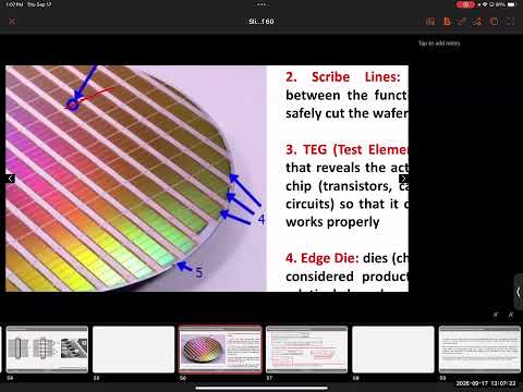
- A silicon wafer repeats the same chip pattern across its surface; modern wafers are commonly about 300 mm in diameter.
- Scribe lines leave space for cutting individual dies, while test element groups (TEGs) provide structures for checking process and circuit behavior before packaging.
- Because a circular wafer is patterned uniformly, dies at its curved edge are often incomplete and discarded; a flat or notch also helps with handling and orientation.
12:10
Fixed Costs, Variable Costs, and Chip Economics
- Variable cost per IC includes the wafer and fabrication, testing, packaging, and final test; fixed costs include building and equipping a foundry.
- High production volume spreads fixed investment across more chips, which is why large markets such as smartphones can support expensive fabrication facilities.
- Automated wafer handling reduces routine manual contact, but the robots, equipment, and clean-room facilities contribute to the large upfront cost.
18:18
Scaling, Yield, and 200 mm versus 300 mm Wafers
- Shrinking transistor and chip area can fit more dies on a wafer, reducing cost per usable chip when yield remains healthy.
- Yield is the percentage of fabricated dies that work; adding process complexity can reduce yield even when individual devices perform better.
- Moving from 200 mm to 300 mm wafers increases the number of potential dies per wafer, but edge losses and process defects still affect the usable total.
24:28
From CMOS Inverter Schematics to Physical Structure
- The fabrication discussion starts with the CMOS inverter, pairing an NMOS and PMOS as the foundation for understanding digital logic.
- A transistor has source, gate, drain, and body terminals, but all circuit connections must be accessed from the wafer’s top surface.
- A physical MOSFET layout therefore represents structures formed through top-down processing rather than the side-view transistor symbols used in circuit diagrams.
28:33
P-Type Substrates, N-Wells, and Ohmic Contacts
- Starting with a p-type silicon substrate makes NMOS formation direct: heavily doped n-type source and drain regions are formed in the p-type body.
- A PMOS requires an n-type body, so it is made inside an n-well formed within the p-type substrate.
- Localized N+ or P+ regions improve metal-to-semiconductor contacts by making them more ohmic and less resistive than contacts to lightly doped material.
34:18
Doping Interfaces and NMOS–PMOS Isolation
- The band-diagram comparison explains why a heavily doped N+ region contacting an N region has a smaller barrier than a junction between different conductivity types.
- NMOS and PMOS regions are separated by insulating oxide so neighboring devices do not become electrically shorted.
- An n-well occupies additional layout area around PMOS devices, so NMOS and PMOS structures are not geometrically identical.
38:25
Why CMOS Layouts Use a Top View
- The layout view groups PMOS devices in an n-well and places NMOS devices in the surrounding p-type substrate, with oxide isolation between regions.
- Wafer processing such as diffusion, etching, and deposition accesses the surface from above; proposed device structures must be manufacturable from that direction.
- This process constraint is why designers work with top-view layouts in Cadence Virtuoso even when the device itself has a three-dimensional structure.
43:20
Reading an Inverter Layout and Its Contacts
- In the CMOS inverter layout, the PMOS connects toward VDD, the NMOS connects toward ground, their gates share the input, and their joined source/drain node forms the output.
- Metal-to-semiconductor connections use contacts, with N+ or P+ regions helping create low-resistance connections.
- Multiple contacts can provide redundancy: electromigration can gradually degrade metal connections, and a failed single contact can disconnect a circuit.
51:35
Metal Layers, Vias, and Interlayer Dielectrics
- Dense circuits use stacked interconnect layers—such as Metal 1, Metal 2, and Metal 3—to route connections that cannot fit in one plane.
- Insulating interlayer dielectric separates metal levels; vias connect selected wires across layers.
- Adjacent metal wires create parasitic capacitance that can cause delay and coupling, so low-k dielectric materials help reduce interlayer capacitance.
56:29
From Silicon Wafer to Packaged Chip
- The fabrication overview traces wafer production from purified silicon through a cylindrical crystal, wafer slicing, and chemical-mechanical polishing.
- Repeated deposition, patterning, doping, and polishing steps build transistor structures and metal interconnects across the wafer.
- Dies are tested, cut apart along scribe lines, and packaged; the packaged chip, rather than the bare die, is the product typically sold.
1:02:16
Silicon Oxide, Photoresist, and Mask Exposure
- Heating silicon forms a silicon dioxide layer with a useful interface to silicon, a material advantage that helped establish silicon as the dominant semiconductor platform.
- Photoresist is spun across the wafer to make a uniform coating; positive and negative resists respond differently to light exposure.
- A patterned mask controls where light reaches the photoresist, transferring a circuit pattern onto the wafer.
1:08:54
Etching and Dopant Diffusion Form an N-Well
- After exposure, a developer removes selected photoresist; a separate etchant removes exposed silicon dioxide, and the remaining resist is stripped to leave an opening.
- N-type dopants enter the exposed p-type silicon and compensate for its original doping, creating an n-well rather than bonding in a separately fabricated piece.
- Dopant dose and exposure time influence penetration depth and well dimensions; diffusion can produce a concentration gradient, and the same masked process repeats across the wafer.
Summary, takeaways, and chapters were generated by AI from the video's transcript and may contain errors. The video belongs to its creator, NorDIC Lab.