ECE1756_lecture9_part2_2026_ram_blocks
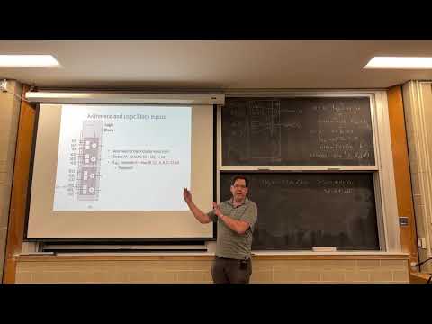
Overview
Vaughn Betz explains how Altera’s adaptive logic modules combine fracturable LUTs with carry-chain adders, then shows how FPGA CAD tools map logical memories onto physical block RAMs. The lecture connects architectural choices such as RAM width, depth, and port count to concrete costs, including a 200-fold density advantage for dedicated RAM over logic-built storage and the duplication required for extra read ports.
Key takeaways
- Altera ALMs can produce two arithmetic bits by routing internal four-input LUT outputs into two adders, reusing LUT and register resources already present in the logic element.
- A memory built from FPGA registers and LUTs is highly flexible but inefficient: a 1 KB, 256-by-32 RAM takes about 6,000 ALMs, compared with roughly 28 ALMs of area for a similar 9-kilobit Stratix IV block RAM.
- Logical RAM mapping can combine physical blocks in parallel for width, in groups for depth, and with output muxes for address selection; extra independent read ports usually require replicated storage.
- Block RAM access consumes power even when read data is ignored, so read-enable signals should disable unselected RAM groups in depth-expanded memories.
- SRAM port count is an architectural area tradeoff: a dual-port cell grows from six to eight transistors and also needs duplicated decoders and peripheral circuits.
- Configurable RAM width reduces shape mismatch, while larger blocks improve area per bit by amortizing peripheral circuitry; choosing block granularity balances density against wasted capacity.
Chapters
- Recent Altera devices use six-input LUT structures that can be viewed as four internal four-input LUTs feeding arithmetic circuitry.
- An adaptive logic module can use those LUT pieces to feed two adders, producing two bits of arithmetic per ALM.
- Altera provides registers for the resulting sum outputs, reusing resources otherwise available for LUT outputs.
- Betz contrasts this with Xilinx fracturable six-LUT structures, which provide one arithmetic bit per LUT in the cited design.
- Two-bit addition fits an ALM using four data inputs, with each four-LUT forwarding one operand bit to an adder.
- A runtime add/subtract function XORs each B bit with a shared control; the carry-in is set by the same add/subtract convention.
- Adding either B or C to A uses seven inputs across two bits, including a shared select signal, and fits within the ALM’s eight-input capacity.
- Selecting between two operand pairs before addition can exceed the eight-input budget when both arithmetic bits and their controls are counted.
- An ALM may support eight inputs, but an Altera logic block with ten ALMs provides only 52 shared inputs rather than 80 independent inputs.
- For a 20-bit addition of A to either B or C, the data and select signals can require 61 inputs, exceeding that block-level limit.
- Altera adds a carry-chain mux that can continue from halfway through a logic block or from its end, allowing a chain to use only ten ALMs when inputs are scarce.
- The unused ALMs can still support other logic with remaining block inputs, while the dedicated carry wiring preserves fast propagation between blocks.
- FPGA memories serve as FIFOs, clock-domain buffers, scratchpads for packet headers, coefficient stores, soft-processor program memory, and register files.
- Building a 1 KB memory organized as 256 words by 32 bits requires 8,192 registers, an address decoder, and 32 separate 256-to-1 read muxes.
- That register-and-logic implementation takes about 6,000 ALMs, while a comparable 9-kilobit Stratix IV RAM occupies area equivalent to about 28 ALMs.
- The dedicated RAM is roughly 200 times denser, making block RAMs essential once memories grow beyond very small sizes.
- FPGA architects choose physical RAM capacity, port width, and port count, from a single-port read-or-write design to multiple simultaneous read/write ports.
- Some FPGAs also provide LUT RAM, which repurposes LUT SRAM cells as writable memories rather than read-only lookup tables.
- Designers describe logical RAMs in RTL or IP, while CAD tools map those requested dimensions and ports onto the physical blocks available on the chip.
- The assignment example uses a physical 8-kilobit RAM organized as 1,024 words by 8 bits with one read port and one write port.
- The target logical RAM has 2,048 words of 32 bits, two independent read ports, and one write port.
- Four 1,024-by-8 physical RAMs operate in parallel to produce each 32-bit word, sharing the same read and write addresses.
- The physical blocks have only 1,024 words, so a second group of four creates the additional depth; the high address bit selects which group receives a write.
- A 2-to-1 mux on each output bit selects the correct 32-bit read word using the high read-address bit.
- A second independent read port requires duplicating the entire constructed memory, including all physical RAM blocks, so each copy can use a separate read address.
- Both copies receive the same write address and write data, keeping their stored contents identical.
- Read-enable signals should disable the unselected depth group, since block RAM reads consume power even when their outputs are discarded.
- For the example, the mapping uses 16 physical 1,024-by-8 RAM blocks: eight per read-port copy.
- High-port-count memories are expensive in FPGAs because additional read ports often require replicated storage; extra write ports are even more costly.
- Designers can reduce port pressure by distributing storage or scheduling accesses across cycles rather than using a heavily ported central memory.
- Double pumping can provide two accesses per design cycle when block RAM runs at twice the design clock, such as 800 MHz RAM serving a 400 MHz design.
- Time-multiplexing a faster RAM requires supporting logic and clock coordination, but can avoid duplicating the entire memory.
- A standard SRAM cell uses six transistors: cross-coupled inverters store a bit, and access transistors connect it to complementary bit lines.
- During a read, the word line activates the access transistors and the stored state pulls the two precharged bit lines apart without flipping the cell.
- During a write, strong drivers force opposite values onto the bit lines and overpower the storage cell to change its state.
- Reliable read and write behavior depends on careful transistor sizing, a challenge that becomes harder as process geometries shrink.
- An SRAM array organizes cells into rows and columns, with each word line activating a row and each bit-line pair carrying one stored bit.
- A row decoder selects the addressed word line, while a differential sense amplifier detects which bit line is higher after a small voltage difference develops.
- Sense amplifiers can resolve a difference of about 30 millivolts, so internal timing waits for the bit lines to separate sufficiently.
- Write drivers force bit-line values during writes; during reads, circuitry precharges both bit lines to approximately VDD/2.
- A dual-port SRAM cell adds a second word line, access-transistor pair, and bit-line pair, allowing two addresses to be read concurrently.
- The extra access path raises the storage cell from six to eight transistors and requires a second decoder and another set of read/write peripheral circuits.
- Simultaneous writes to the same cell with different data have undefined behavior; read-during-write behavior may return old data, new data, or unspecified data.
- FPGA RAM configuration can select old-data or new-data behavior by adjusting internal timing, while the unspecified option is generally faster.
- Larger RAMs reduce area per bit because peripheral circuitry is amortized; the assignment model includes bit-proportional area, square-root-proportional peripheral area, control overhead, and routing ports.
- Oversized RAM blocks can waste capacity when a design needs only a small buffer, and mismatched width or depth can leave usable bits stranded.
- Configurable-width block RAMs reshape a core such as 1,024 words by 8 bits into configurations such as 2,048 by 4, 4,096 by 2, or 8,192 by 1 using muxes and address bits.
- Block RAM inputs are registered to support internal self-timed decoding and sensing; output registers are often optional, and muxing can adjust the apparent width and depth.
Transcript excerpt
0:00 again. Um, okay. So, you saw this trick then of going, you know, breaking the lookup table up into its pieces using them to feed uh the adders so that we can do a bit more than addition. Uh, and we're re we're not adding routing ports, but we're adding arithmetic. It's a very efficient way to do it. Okay. So, I'm going to show you some examples from well, Intel Altera in their recent devices. So, everything after Stratex 2 is basically the same arithmetic structures. Uh so I was showing you that with a fourllet. Okay, the example I just gave you is take a fourlet. You break it in inside. It's got two three LUTs. We hook the outputs of each of those to the adder. Okay, so Alterara's recent chips actually have six LS. Uh they can already be broken into two five Ls. Um but those two five LUTs inside them have two four LTs. So we can also
0:48 think of it as having four four LUTs uh inside of it. Uh and that's what Alterero does. So they take those four four LUTs and they basically pull a signal. You know, when you're using this as a as normal lookup tables, you have more muckses that I'm not showing to do the five L or the sixlet function here. I'm showing you just taking signals out of the four LUTs that are inside there. And I'm feeding, you know, those signals in pairs to my adders. So I can actually build two bits of addition for an adaptive logic module. Um, if I build two bits of addition, things work out pretty well. I basically take a fourlet feed one input, fourlet feed the other input that I'm adding, and do the same thing down here. So, that's fine. I
This is the start of the transcript. Save this video free for the whole transcript, searchable and time-coded.
In this course
Related notes
Summary, takeaways, and chapters were generated by AI from the video's transcript and may contain errors. The video belongs to its creator, Vaughn Betz.