The Closest Thing We Have to Alien Technology
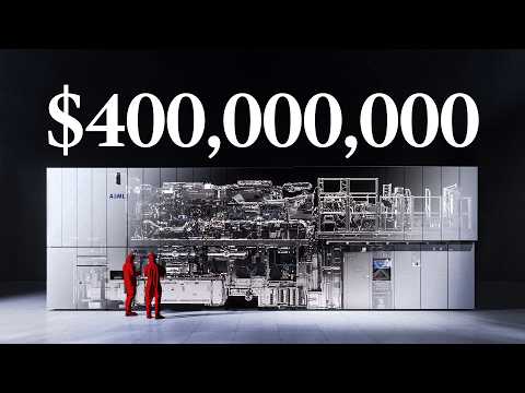 Watch on YouTube →
Overview
ASML’s extreme ultraviolet lithography (EUV) machines use laser-driven tin plasma and atomically smooth Zeiss mirrors to print chip features small enough to keep Moore’s Law advancing after conventional lithography stalled around 2015. The machines took more than three decades to develop, combining a 13.5-nanometer light source, precisely controlled optics, and layer alignment around one nanometer; their engineering story also shows how researchers and companies persisted through technical failures, skepticism, and shifting commercial requirements.
Key takeaways
- EUV overcame the wavelength limits of 193-nanometer lithography by using 13.5-nanometer light, enabling smaller chip patterns with a manageable combination of light source and mirror reflectivity.
- An EUV machine’s light budget is extremely tight: nine surfaces reflecting about 70% each leave only around 4% of the original light, making source power essential to commercial throughput.
- ASML’s laser-produced tin plasma works by shaping droplets with successive pulses; modern sources use three pulses to condition and ionize each target and produce roughly 500 watts of EUV light.
- EUV mirrors must be both exceptionally smooth and actively stabilized: high-NA optics combine near-atomic surface quality with controls that compensate for heat-driven shifts.
- ASML’s commercial breakthrough required more than solving the optics: hydrogen and oxygen management, debris control, high-speed droplet tracking, and sustained production rates all had to work together.
- EUV’s path from early experiments to chip manufacturing took about 30 years, illustrating how long-term research partnerships and persistent investment can turn a repeatedly doubted idea into essential infrastructure.
Chapters
0:00
Moore’s Law Meets the $400 Million EUV Machine
- For decades, transistor counts roughly doubled every two years, but progress slowed around 2015 as 193-nanometer lithography approached its limits.
- ASML’s EUV machine fires laser pulses at 50,000 tin droplets per second, heating them above 220,000 kelvin to produce extreme ultraviolet light.
- The system’s mirrors are extraordinarily smooth, and its chip-layer alignment can be accurate to about five silicon atoms.
3:13
How Silicon Wafer Layers Are Printed with Light
- Chip manufacturing begins with ultrapure silicon crystal ingots, which are sliced into wafers and polished before processing.
- Photolithography repeatedly coats, exposes, etches, and deposits material to build chips with roughly 10 to 100 layers.
- Diffraction makes small mask features difficult to resolve; the Rayleigh equation links printable feature size to light wavelength and numerical aperture.
9:14
Hiroo Kinoshita’s EUV Idea and the Challenge of X-Ray Mirrors
- In the 1980s, Hiroo Kinoshita proposed using roughly 10-nanometer light to print finer chip features than 193-nanometer deep-UV systems could manage.
- EUV light is absorbed by air and ordinary lenses, requiring a vacuum system that uses reflective optics instead.
- Jim Underwood and Troy Barbee demonstrated multilayer x-ray mirrors; Kinoshita later used tungsten-carbon mirrors to print 4-micron lines with 11-nanometer light.
- The mirrors had to be atomically smooth: Kinoshita’s work required average surface bumps of only about 2.3 silicon atoms.
15:08
Andrew Hawryluk, Bell Labs, and the First EUV Lithography Prototype
- Lawrence Livermore National Laboratory developed multilayer mirrors to study x-rays from fusion research, and Andrew Hawryluk proposed applying them to chip lithography.
- After Hawryluk’s proposal was ridiculed at a conference, Bell Labs and national laboratories joined efforts to develop the technology.
- The project was named extreme ultraviolet lithography, or EUV; when US government funding was cut in 1996, Intel, Motorola, AMD, and others invested $250 million to continue it.
- The 2000 Engineering Test Stand produced 9.8 watts of 13.4-nanometer light and printed 70-nanometer features, proving EUV could work.
19:56
Why the EUV Prototype Could Not Yet Make Chips at Scale
- The Engineering Test Stand printed only about 10 wafers per hour, far below the hundreds per hour needed for commercial production.
- Each of its nine reflective surfaces retained about 70% of the light, leaving only around 4% to reach the wafer.
- A practical system needed more source power, but using fewer mirrors would worsen optical aberrations; modern systems use six mirrors to manage them.
- Most US companies eventually withdrew from full machine development, leaving ASML as the main industrial champion.
22:03
ASML and Zeiss Choose 13.5-Nanometer Light and Tin Plasma
- ASML partnered with Zeiss, which developed the mirrors, while ASML focused on creating a sufficiently powerful EUV source.
- Silicon-molybdenum multilayer mirrors offered up to about 70% reflectivity near 13 nanometers; a higher-reflectivity beryllium option was rejected because it is toxic and difficult to handle.
- ASML moved from discharge-produced plasma to laser-produced plasma after the simpler source stalled at a few watts.
- Tin emits strongly near 13.5 nanometers and can be converted to EUV more efficiently than xenon, but its droplets must be precisely formed and timed.
30:02
Tin Debris, Hydrogen Shockwaves, and Nanometer-Controlled Mirrors
- Tin contamination threatened the collector mirror, so low-pressure hydrogen slows debris and reacts with deposited tin to form stannane gas.
- Laser-driven plasma events create repeatable shockwaves in hydrogen; the Taylor–von Neumann–Sedov formula helped engineers calculate the required gas flow, reaching about 360 kilometers per hour.
- As source power rose, heat shifted the optics, so Zeiss added sensors and controls to stabilize mirror positions and angles at nanometer and picoradian scales.
- By 2013, ASML reached 50 watts, but neutral tin still absorbed EUV light and debris limited source performance.
37:07
The Two-Pulse Tin Target Breakthrough Reaches 200 Watts
- ASML’s breakthrough used a pre-pulse to flatten each tin droplet into a pancake before a stronger pulse vaporized it into plasma.
- The larger, thinner target improved EUV production without adding the same burden of debris or neutral atoms.
- ASML reached 100 watts in 2014, then had to push to 200 watts and 125 wafers per hour as competing 193-nanometer multi-patterning improved.
- Laser curtains track droplets through turbulent hydrogen flow and time the main pulse; ASML demonstrated 200 watts in 2015.
41:01
High-NA EUV: 500-Watt Sources, 20-G Scans, and Five-Atom Alignment
- Adding a controlled amount of oxygen helped keep the collector mirror clean longer, making continuous commercial operation more practical.
- Low-NA machines use a numerical aperture of 0.33; high-NA systems raise it to 0.55 and have printed lines around 8 nanometers wide.
- Current sources use three laser pulses per droplet and reach roughly 500 watts at 60,000 droplets per second, with 100,000 per second demonstrated in the lab.
- A 20,000-watt CO₂ laser powers the source, while the reticle accelerates above 20 G and layer overlay is held to about one nanometer.
49:57
A Global Supply Chain and the Case for Unreasonable Persistence
- A high-NA machine depends on about 5,000 suppliers and 100,000 parts, including 3,000 cables, 40,000 bolts, and two kilometers of hosing.
- Shipping one machine requires about 250 containers, 25 trucks, and seven Boeing 747s.
- EUV took roughly three decades to move from Kinoshita’s early experiments to manufacturing, despite repeated failures and skepticism.
- The closing argument is that progress often depends on people willing to pursue technically unreasonable ideas, even when experts identify strong reasons they may fail.
52:57
Brilliant Sponsorship: Learning Through Interactive Science
- The closing sponsorship presents Brilliant as an interactive platform for learning math, science, and computer science through practice.
- Its Scientific Thinking course is recommended for breaking complex engineering ideas, such as optics, into smaller concepts.
- The segment offers a 20% discount on an annual Premium subscription through the Veritasium link.
Summary, takeaways, and chapters were generated by AI from the video's transcript and may contain errors. The video belongs to its creator, Veritasium.